1. Software & Firmware Configuration (nRF Connect SDK)
2. Optimize Bluetooth LE (BLE)
2.1. Case Study Analysis
2.2. Optimizing Connection Parameters
2.3. Solutions proposed through experimentation
3. Hardware Design Optimization
4. Measurement and Fault Correction Procedure
Optimizing the power consumption of nRF series devices (nRF52, nRF53, nRF91) down to microampere levels requires a combination of hardware design, firmware configuration, and protocol optimization. Below are the detailed steps to achieve ultra-low power consumption.
1. Software & Firmware Configuration (nRF Connect SDK)
This is a fundamental step to ensure that the operating system (Zephyr RTOS) and peripherals do not consume excessive power.
- Disable Serial Logging (UART): UART consumes a significant amount of battery power (~1.2mA). Completely disable it in the prj.conf file when releasing the product.
Code snippet
CONFIG_SERIAL=n
CONFIG_UART_CONSOLE=n
CONFIG_LOG=n
Blinky with Logging ON (~470 uA).
Blinky with Logging OFF (~6 uA).
- Enable Power Management: Allows Idle Threads to put the CPU into a sleep state.
Code snippet
CONFIG_PM=y
CONFIG_PM_DEVICE=y
- Turn on the DC/DC converter: Using a DC/DC converter instead of an LDO can reduce power consumption by up to 35%.
Code snippet
CONFIG_BOARD_ENABLE_DCDC=y- Optimize RAM Retention: Only retain necessary RAM during sleep mode. The fewer RAM regions retained, the lower the static current.
- Use App Timers: Absolutely do not use nrf_delay_ms() (CPU loop). Use k_timer to keep the CPU completely idle and enter Sleep mode.
2. Optimize Bluetooth LE (BLE)
The frequency and power of the transmission determine the battery life of sensor-based communication applications.
2.1. Case Study Analysis
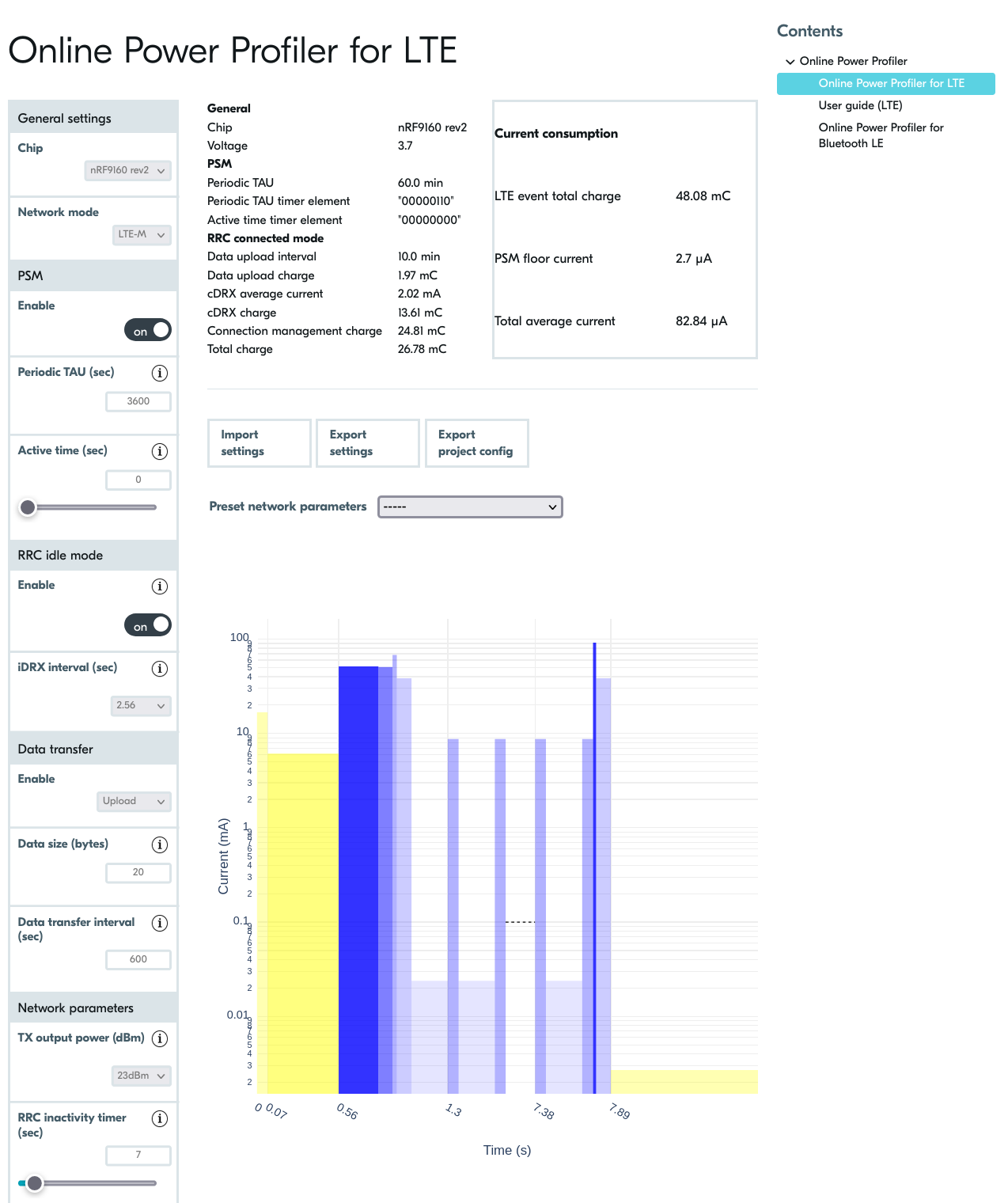
Before deploying the hardware, we used Nordic’s Online Power Profiler (OPP) tool to estimate power consumption. The image shows a simulation of the nRF9160 device running LTE-M with an ideal idle current (PSM Floor) of 2.7 µA. This helps establish a target ‘milestone’ for the firmware engineering team to aim for during real-world optimization.
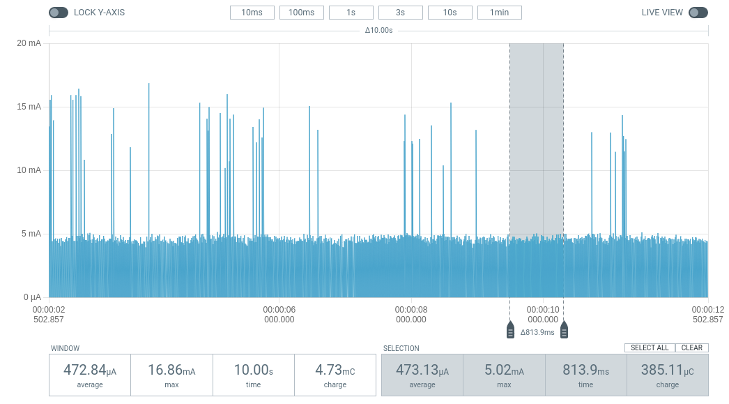
Through practical measurements using PPK2, we can clearly see the difference between optimization and non-optimization:
- Scenario 1: Firmware is not optimized (mA base current)
- Average current: 1.71 mA.
- Symptom: BLE pulses are stable, but the background current between pulses does not decrease (because the CPU or peripherals remain ON).
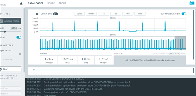
The BLE device operates at a 1-second cycle but is not yet optimized for Sleep Mode, with the average current remaining high at 1.71 mA.
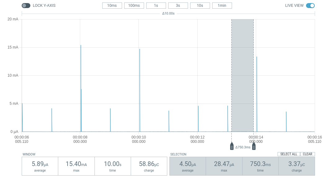
- Scenario 2: After optimization (Background line µA)
- Average line: 94.4 µA.
- Efficiency: Despite the dense data transmission cycle (30ms), the average current is reduced by 18 times thanks to the chip’s excellent deep sleep function between connection cycles.
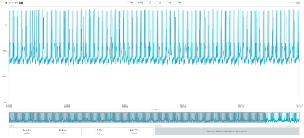
After complete firmware optimization, the device’s average current dropped to 94.4 µA even with a short connection cycle of 30ms.
2.2. Optimizing Connection Parameters
- TX Power: Increasing from 0dBm to +4dBm consumes an additional 2.2mA but significantly increases range. If the distance is short, consider reducing TX Power to -4dBm to save battery power.
- Peripheral Latency: Allows the device to skip connection cycles when there is no new data, extending sleep time without disconnection.
2.3. Solutions proposed through experimentation
- For hardware:
- System Resource Management:
- Disable Logging (UART/RTT): When UART is active, it prevents the MCU from entering low power consumption mode. In a production environment, completely disabling NRF_LOG can immediately save 1.2 mA.
- Enable Internal DCDC: Instead of using the default LDO voltage regulator, configuring the internal DC-DC converter will significantly improve power efficiency when the radio is running.
sd_power_dcdc_mode_set(NRF_POWER_DCDC_ENABLE);
- System Resource Management:
- For software:
- Optimizing GPIO and Peripheral State
- Floating Pins: GPIO pins that are not configured to float can cause unspecified leakage current. The golden rule is to put unused pins to the Input Disconnect state.
- Uninit Peripherals: Always unplug (Uninit) peripheral modules such as ADC, SPI, and I2C immediately after data sampling is complete.
- Leverage Low Power Mode in Firmware; instead of using traditional wait loops, use event-driven processing:
- Use the __WFE() (Wait For Event) instruction to put the CPU into sleep mode.
- Utilize RTC (Real-Time Counter) instead of high-frequency timers for recurring tasks.
- Optimizing GPIO and Peripheral State
3. Hardware Design Optimization
- External crystal oscillator (LFCLK 32kHz): Using an external crystal oscillator instead of an internal one saves 2-10% energy due to higher accuracy, reducing the chip’s “wake-up” time to compensate for time discrepancies (clock jitter).
| Symbol | Description | Min. | Typ. | Max. | Units |
|---|---|---|---|---|---|
| fNOM_LFCLK |
Nominal output frequency |
32.768 | kHz | ||
| tSTART_LFXO |
Startup time for 32.768 kHz crystal oscillator |
0.43 | s | ||
| fTOL_LFRC |
Frequency tolerance, uncalibrated |
±4.5 | % | ||
| fTOL_CAL_LFRC |
Frequency tolerance after calibration. Constant temperature within ±0.5 °C, calibration performed at least every 8 seconds, averaging interval > 7.5 ms, defined as 3 sigma. |
±250 | ppm | ||
| tSTART_LFRC |
Startup time for internal RC oscillator |
1000 | μs |
- DC/DC Component Activation: To achieve a 35% reduction in current consumption, the hardware must have suitable inductors and capacitors for the internal DC/DC converter.
- Sensor Leakage Management: For external sensors with high leakage current in standby mode, design an additional Load Switch (P-channel MOSFET) to completely cut off power to the sensor when the chip enters the SYSTEM_OFF state.
- Operating Voltage: The nRF52 is optimized at 3V. Running at a lower voltage does not necessarily reduce core current consumption, but significantly impacts the performance of GPIOs and peripherals.
4. Measurement and Fault Correction Procedure
- Exiting Debug Mode (DIF Mode): A classic mistake is measuring current immediately after programming without disconnecting the programmer. The nRF chip will keep the debug ports open and consume hundreds of mA. Solution: Always power cycle (disconnect and reconnect power) and disconnect the SWD cable before measuring the final current.
- Isolate the measurement source: Ensure the measurement circuit only powers the nRF SoC. If the power supply is shared between the LED, sensor, or programmer, the mA measurement will never accurately reflect the chip’s current.
- Use specialized measurement tools: Use the PPK2 in Ammeter mode to clearly see the electrical pulses. Avoid using a regular multimeter as they lack the sampling rate to capture extremely short BLE pulses.
Compare practical effectiveness: