Enterprise-Grade Thread OTA Updates on nRF52840
1. Analysis of embedded hardware and operating system architecture
1.1. Nordic nRF52840 SoC Hardware Architecture
1.2. Zephyr RTOS Real-Time Embedded Operating System
2. OpenThread Border Router (OTBR) Network Infrastructure
2.1. Initialize the Border Router
2.2. Synchronize network parameters (Dataset)
2.3. Terminal Routing (Commissioning)
3. Secure Authentication and Boot Mechanism with MCUboot
4. Firmware Update Procedure via MCUMGR Protocol
5. Practical Project Implementation and Hardware Ecosystem
1. Analysis of embedded hardware and operating system architecture
1.1. Nordic nRF52840 SoC Hardware Architecture
The Nordic nRF52840 microcontroller on the Seeed Studio XIAO BLE board is the optimal hardware solution for end-devices in the Smart Home ecosystem. This chipset features a 2.4 GHz multi-protocol radio transceiver, supporting both IEEE 802.15.4 (the foundation of Thread networks) and Bluetooth Low Energy (BLE). This allows programmers to use BLE to configure network commissioning via phone, then transfer data streams to the Thread network for stable operation and battery saving.
Inside the chip, the ARM Cortex-M4 (64 MHz) central processing core provides powerful performance to simultaneously run heavy protocol stacks such as OpenThread. Notably, the ARM TrustZone CryptoCell-310 hardware encryption accelerator acts as a dedicated security shield. This block automatically handles encryption algorithms (AES-CCM), data hashing (SHA-256), and digital signature authentication of MCUboot without consuming CPU resources, optimizing energy and protecting the device from the risk of hijacking or flashing pirated firmware.
1.2. Zephyr RTOS Real-Time Embedded Operating System
The nRF52840’s hardware infrastructure is managed by Zephyr RTOS – a dedicated real-time operating system for IoT systems, thanks to its flexible hardware abstraction capabilities through two tools:
- Devicetree (DTS): Describes the physical hardware structure (GPIO pins, UART, Flash partition for MCUboot) in a tree structure, allowing hardware configuration changes to be independent of the application source code.
- Kconfig: A compile-time feature selector that enables/disables software modules (e.g., CONFIG_BOOTLOADER_MCUBOOT=y) using intuitive configuration flags.
2. OpenThread Border Router (OTBR) Network Infrastructure
2.1. Initialize the Border Router
Establish a gateway to convert packets between a local IPv6 network (Wi-Fi/Ethernet) and a low-power wireless Thread network using a Raspberry Pi 5 in conjunction with the SONOFF Dongle Plus MG24 acting as a Radio Co-processor (RCP).
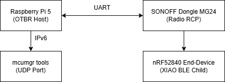
This model shows the physical connection between the Host Controller (Raspberry Pi 5) and the RCP radio circuit (SONOFF Dongle Plus MG24) via USB-UART communication.
2.2. Synchronize network parameters (Dataset)
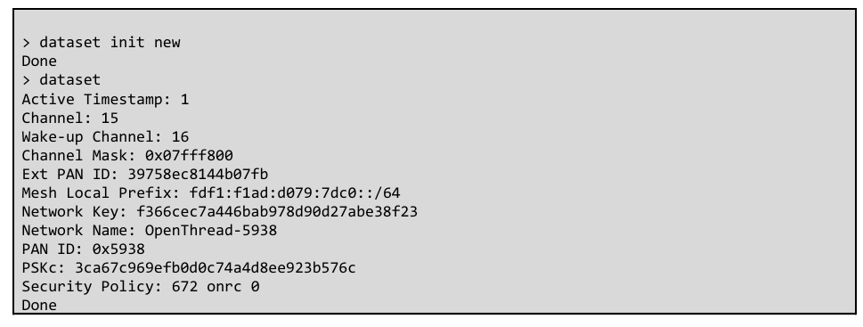
Configure the Active Dataset identifier parameters, including Network Key, PAN ID, Extended PAN ID, and Channel Mask, via the ot-ctl system controller.
2.3. Terminal Routing (Commissioning)
The process involves scanning for signals (ot discover), verifying the data configuration, and establishing the child connection state of the nRF52840 SoC (Seeed Studio XIAO BLE) into the network topology.
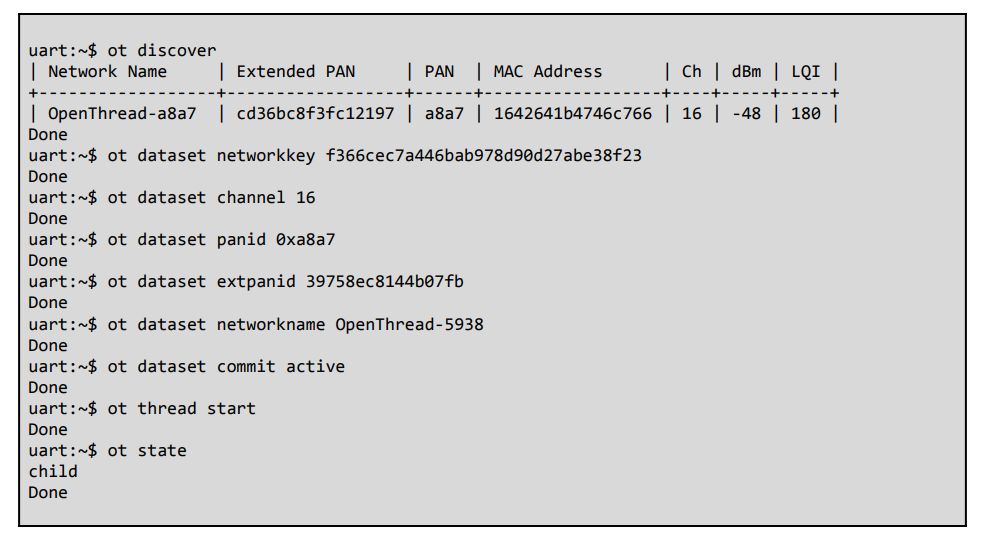
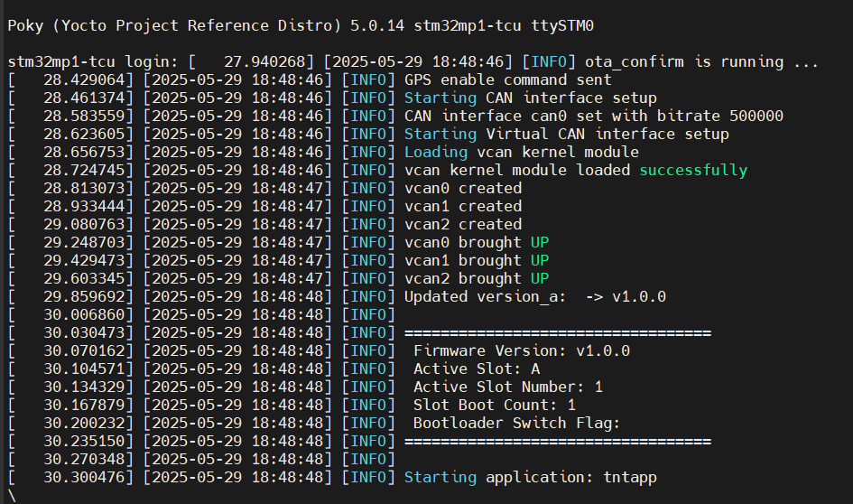
nRF52840 Thread commissioning and connection log via Zephyr Shell
3. Secure Authentication and Boot Mechanism with MCUboot
In the security architecture of IoT devices, the MCUboot acts as the first line of defense when the device is powered on. Before transferring control to the main application, MCUboot verifies the integrity and authenticity of the firmware stored in Flash memory. This process uses asymmetric encryption algorithms (such as RSA or ECDSA): MCUboot decrypts and compares the digital signature attached to the end of the application file with the public key embedded in the bootloader’s source code. If the hash (SHA-256) matches and the digital signature is valid, the device is allowed to boot; otherwise, the system will refuse execution to absolutely prevent the loading of pirated firmware or malware over the network.
To implement a system-free update mechanism and prevent circuit crashes (Anti-bricking), Zephyr RTOS uses a multi-image virtualization hardware structure via the Devicetree Overlay configuration file. This structure divides the internal Flash memory of the nRF52840 SoC into strictly functional partitions, ensuring that OTA data reception and application execution occur in two separate spaces.
┌────────────────────────────────────────────────────────┐
│ nRF52840 INTERNAL FLASH MEMORY │
├────────────────────────────────────────────────────────┤
│ boot_partition (MCUboot Bootloader) │
├────────────────────────────────────────────────────────┤
│ slot0_partition (Active Application – Primary) │
├────────────────────────────────────────────────────────┤
│ slot1_partition (OTA Download Buffer – Secondary) │
├────────────────────────────────────────────────────────┤
│ scratch_partition (Data Swap Space) │
├────────────────────────────────────────────────────────┤
│ storage_partition (Non-Volatile Storage – NVS) │
└────────────────────────────────────────────────────────┘
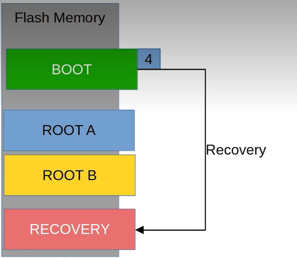
The system decomposes and coordinates these partitions using a secure swap mechanism:
- boot_partition: A fixed partition at the beginning of the memory range, containing the unique executable source code of the MCUboot. This memory area is configured with hardware locking to prevent any overwriting from the application layer.
- slot0_partition (Primary/Active Slot): The partition containing the currently running firmware image. The microcontroller core only reads and executes code directly from this partition.
- slot1_partition (Secondary/Upgrade Slot): A dedicated buffer partition. When the mcumgr tool performs an image upload command over the Thread network, the entire new binary file (app_update.bin) is segmented and gradually written to this partition, without affecting the application running in slot 0.
- scratch_partition: A secondary partition with a minimum size (usually the size of a Flash sector). This memory area acts as an intermediate space to temporarily back up data during the block-by-block swap process between slot 0 and slot 1 after receiving a reset command. This mechanism ensures that if the device suddenly loses power during firmware swapping, the MCUboot can still restore the data to its original state without damaging the chip.
4. Firmware Update Procedure via MCUMGR Protocol
- Network address identification: Use the End-Device’s Mesh-Local EID (IPv6) and default service port (UDP Port 1337) to establish the data transmission flow.
- The 4-step process for deploying upgrade commands via SMP (Simple Management Protocol):
- Memory status query (image list): Reads version information and hash index of the current slots on the target device.
- Segment file transfer (image upload): Pushes the digitally signed binary file (app_update.bin) into the slot1_partition buffer.
- Set test flag (image test): Marks the new partition in a temporarily pending state.
- Reboot and configuration finalization (reset & image confirm): Commands the device to reboot over the network; MCUboot performs partition swapping; after the system successfully boots on the new firmware, sends a permanent confirmation command to complete the upgrade cycle.
5. Practical Project Implementation and Hardware Ecosystem
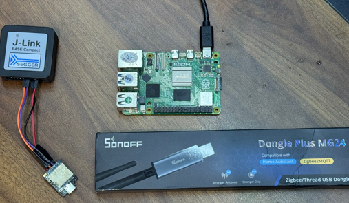
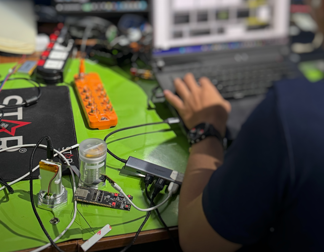
While sections 1 through 4 established the theoretical embedded, network, and security architectures, this section presents the actual physical deployment on the development test bench. Figure 5.1 showcases the integrated hardware ecosystem used for early-stage direct flashing, comprehensive debugging, and subsequent wireless secure over-the-air firmware updates via the Thread network.
Components overview:
- Host Controller (Raspberry Pi): Positioned centrally, this single-board computer is powered via USB-C. It runs the OpenThread Border Router (
ot-br-posix) stack and themcumgrtool, serving as the network gateway and update manager. - Thread RCP Dongle (SONOFF Dongle Plus MG24): Displayed in its commercial packaging (noted for “Compatible with Home Assistant,” “Zigbee2MQTT,” and “Stronger Antenna”), this USB dongle (based on Silicon Labs MG24) will be plugged into the Raspberry Pi. Crucially, it is flashed with the OpenThread Radio Co-processor (RCP) firmware to establish and lead the Thread wireless mesh.
- Debugger (SEGGER J-Link BASE Compact): A high-performance probe connected via a 4-wire SWD/JTAG debugging cable. It is used for initial non-OTA flashing (e.g., programming the MCUboot bootloader) and real-time on-chip debugging of the target device. Its compact form factor is well-suited for embedded development.
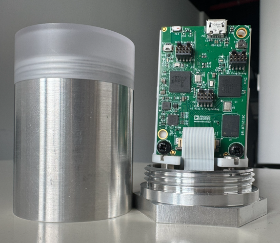
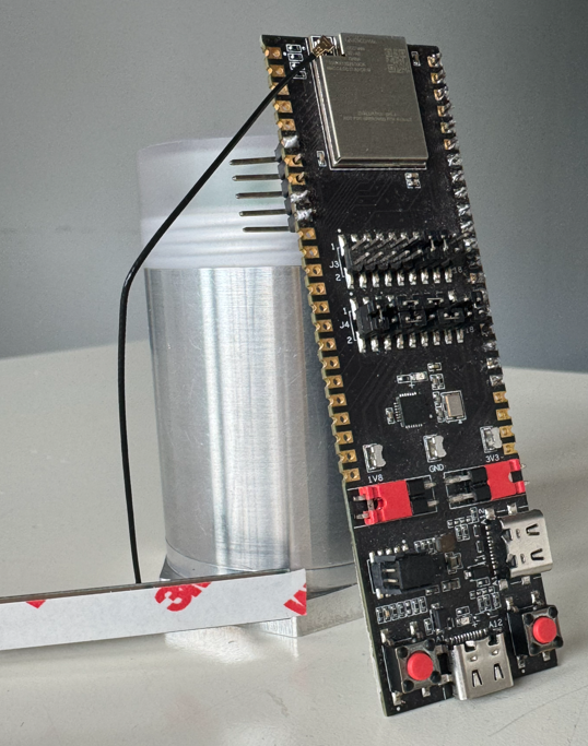
- Target End-Device (nRF52840-based board): The small, metal-shielded nRF52840 module connected to the J-Link probe via the debugging cable. This is the target node for secure OTA updates, and the connection permits RTT console monitoring and direct code execution control.
Practical hardware ecosystem deployed on a wood workbench, showcasing the Raspberry Pi Host Controller, Thread RCP Dongle, SEGGER Debugger, and nRF52840-based Target End-Device. This physical setup demonstrates the end-to-end development workflow: a developer can create code for the nRF52840 SoC, perform initial programming and comprehensive debugging via J-Link, and then transition to a secure deployment phase, managing image updates wirelessly from the Raspberry Pi over the Thread network established by the MG24 dongle, exercising the MCUboot-signed failure-safe update mechanism detailed.
Optimizing nRF Power Consumption: From mA to µA
1. Software & Firmware Configuration (nRF Connect SDK)
2. Optimize Bluetooth LE (BLE)
2.1. Case Study Analysis
2.2. Optimizing Connection Parameters
2.3. Solutions proposed through experimentation
3. Hardware Design Optimization
4. Measurement and Fault Correction Procedure
Optimizing the power consumption of nRF series devices (nRF52, nRF53, nRF91) down to microampere levels requires a combination of hardware design, firmware configuration, and protocol optimization. Below are the detailed steps to achieve ultra-low power consumption.
1. Software & Firmware Configuration (nRF Connect SDK)
This is a fundamental step to ensure that the operating system (Zephyr RTOS) and peripherals do not consume excessive power.
- Disable Serial Logging (UART): UART consumes a significant amount of battery power (~1.2mA). Completely disable it in the prj.conf file when releasing the product.
Code snippet
CONFIG_SERIAL=n
CONFIG_UART_CONSOLE=n
CONFIG_LOG=n
Blinky with Logging ON (~470 uA).
Blinky with Logging OFF (~6 uA).
- Enable Power Management: Allows Idle Threads to put the CPU into a sleep state.
Code snippet
CONFIG_PM=y
CONFIG_PM_DEVICE=y
- Turn on the DC/DC converter: Using a DC/DC converter instead of an LDO can reduce power consumption by up to 35%.
Code snippet
CONFIG_BOARD_ENABLE_DCDC=y- Optimize RAM Retention: Only retain necessary RAM during sleep mode. The fewer RAM regions retained, the lower the static current.
- Use App Timers: Absolutely do not use nrf_delay_ms() (CPU loop). Use k_timer to keep the CPU completely idle and enter Sleep mode.
2. Optimize Bluetooth LE (BLE)
The frequency and power of the transmission determine the battery life of sensor-based communication applications.
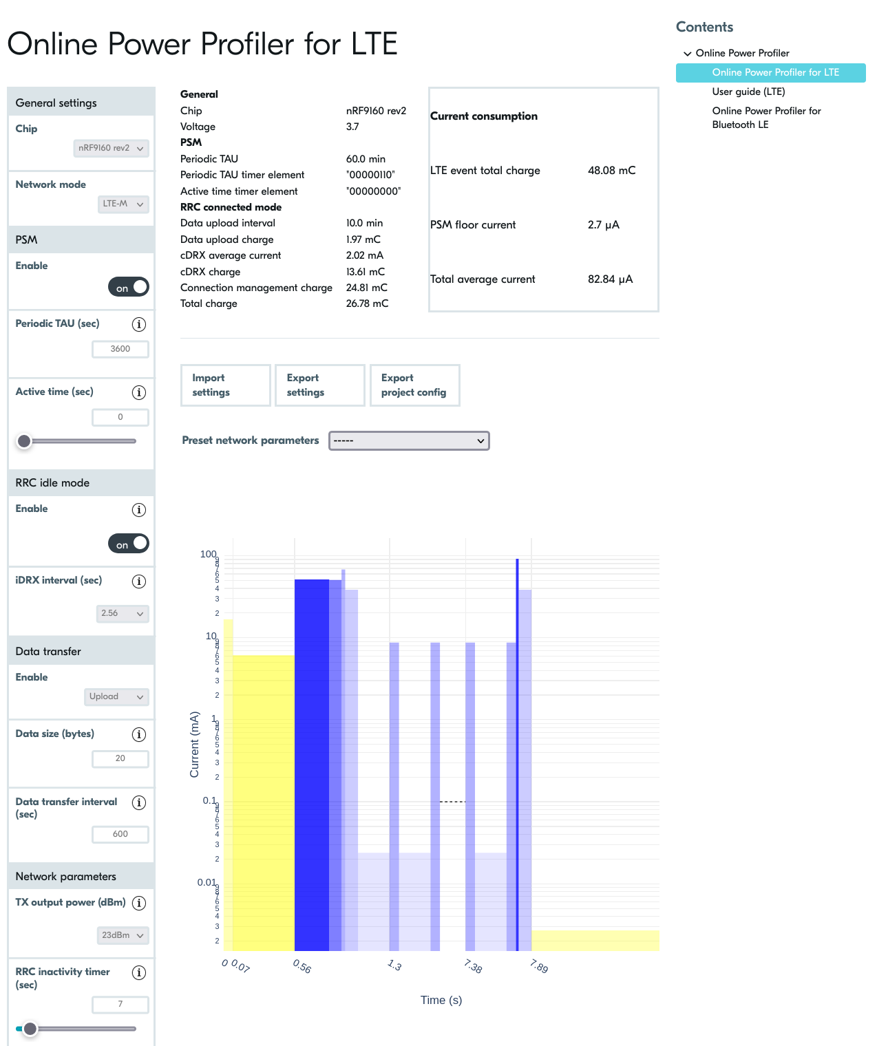
2.1. Case Study Analysis
Before deploying the hardware, we used Nordic’s Online Power Profiler (OPP) tool to estimate power consumption. The image shows a simulation of the nRF9160 device running LTE-M with an ideal idle current (PSM Floor) of 2.7 µA. This helps establish a target ‘milestone’ for the firmware engineering team to aim for during real-world optimization.
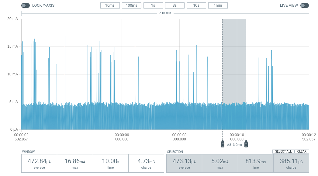
Through practical measurements using PPK2, we can clearly see the difference between optimization and non-optimization:
- Scenario 1: Firmware is not optimized (mA base current)
- Average current: 1.71 mA.
- Symptom: BLE pulses are stable, but the background current between pulses does not decrease (because the CPU or peripherals remain ON).
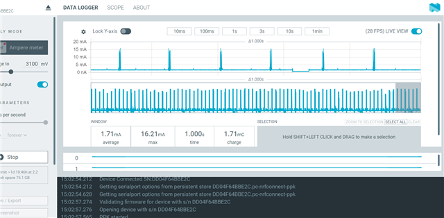
The BLE device operates at a 1-second cycle but is not yet optimized for Sleep Mode, with the average current remaining high at 1.71 mA.
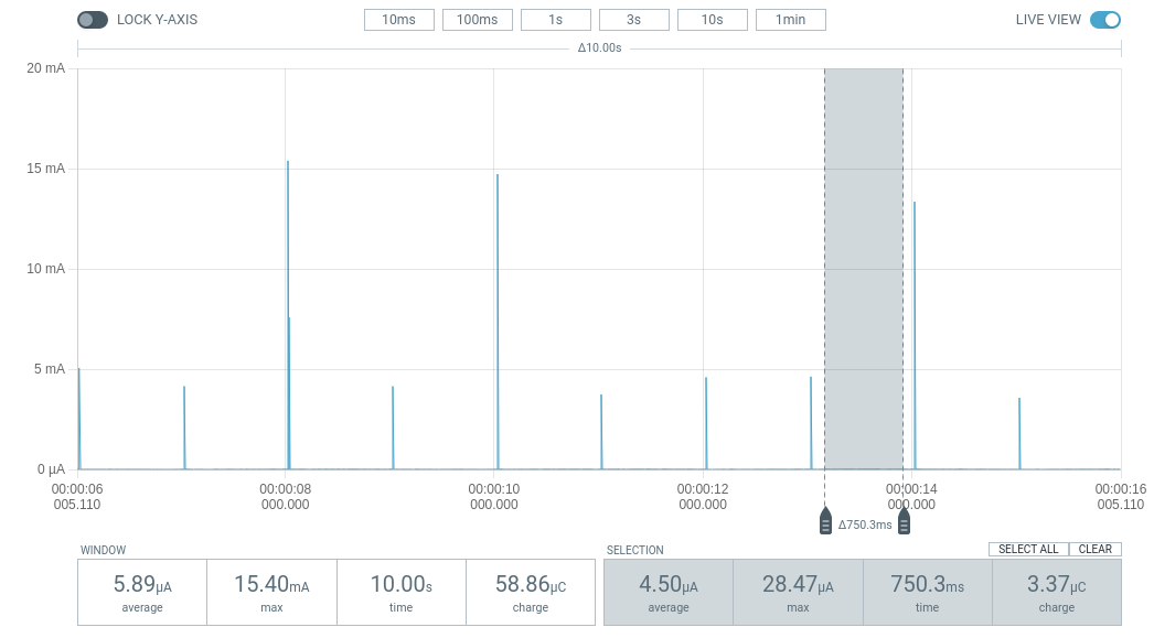
- Scenario 2: After optimization (Background line µA)
- Average line: 94.4 µA.
- Efficiency: Despite the dense data transmission cycle (30ms), the average current is reduced by 18 times thanks to the chip’s excellent deep sleep function between connection cycles.
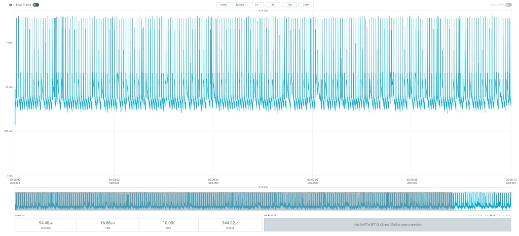
After complete firmware optimization, the device’s average current dropped to 94.4 µA even with a short connection cycle of 30ms.
2.2. Optimizing Connection Parameters
- TX Power: Increasing from 0dBm to +4dBm consumes an additional 2.2mA but significantly increases range. If the distance is short, consider reducing TX Power to -4dBm to save battery power.
- Peripheral Latency: Allows the device to skip connection cycles when there is no new data, extending sleep time without disconnection.
2.3. Solutions proposed through experimentation
- For hardware:
- System Resource Management:
- Disable Logging (UART/RTT): When UART is active, it prevents the MCU from entering low power consumption mode. In a production environment, completely disabling NRF_LOG can immediately save 1.2 mA.
- Enable Internal DCDC: Instead of using the default LDO voltage regulator, configuring the internal DC-DC converter will significantly improve power efficiency when the radio is running.
sd_power_dcdc_mode_set(NRF_POWER_DCDC_ENABLE);
- System Resource Management:
- For software:
- Optimizing GPIO and Peripheral State
- Floating Pins: GPIO pins that are not configured to float can cause unspecified leakage current. The golden rule is to put unused pins to the Input Disconnect state.
- Uninit Peripherals: Always unplug (Uninit) peripheral modules such as ADC, SPI, and I2C immediately after data sampling is complete.
- Leverage Low Power Mode in Firmware; instead of using traditional wait loops, use event-driven processing:
- Use the __WFE() (Wait For Event) instruction to put the CPU into sleep mode.
- Utilize RTC (Real-Time Counter) instead of high-frequency timers for recurring tasks.
- Optimizing GPIO and Peripheral State
3. Hardware Design Optimization
- External crystal oscillator (LFCLK 32kHz): Using an external crystal oscillator instead of an internal one saves 2-10% energy due to higher accuracy, reducing the chip’s “wake-up” time to compensate for time discrepancies (clock jitter).
| Symbol | Description | Min. | Typ. | Max. | Units |
|---|---|---|---|---|---|
| fNOM_LFCLK |
Nominal output frequency |
32.768 | kHz | ||
| tSTART_LFXO |
Startup time for 32.768 kHz crystal oscillator |
0.43 | s | ||
| fTOL_LFRC |
Frequency tolerance, uncalibrated |
±4.5 | % | ||
| fTOL_CAL_LFRC |
Frequency tolerance after calibration. Constant temperature within ±0.5 °C, calibration performed at least every 8 seconds, averaging interval > 7.5 ms, defined as 3 sigma. |
±250 | ppm | ||
| tSTART_LFRC |
Startup time for internal RC oscillator |
1000 | μs |
- DC/DC Component Activation: To achieve a 35% reduction in current consumption, the hardware must have suitable inductors and capacitors for the internal DC/DC converter.
- Sensor Leakage Management: For external sensors with high leakage current in standby mode, design an additional Load Switch (P-channel MOSFET) to completely cut off power to the sensor when the chip enters the SYSTEM_OFF state.
- Operating Voltage: The nRF52 is optimized at 3V. Running at a lower voltage does not necessarily reduce core current consumption, but significantly impacts the performance of GPIOs and peripherals.
4. Measurement and Fault Correction Procedure
- Exiting Debug Mode (DIF Mode): A classic mistake is measuring current immediately after programming without disconnecting the programmer. The nRF chip will keep the debug ports open and consume hundreds of mA. Solution: Always power cycle (disconnect and reconnect power) and disconnect the SWD cable before measuring the final current.
- Isolate the measurement source: Ensure the measurement circuit only powers the nRF SoC. If the power supply is shared between the LED, sensor, or programmer, the mA measurement will never accurately reflect the chip’s current.
- Use specialized measurement tools: Use the PPK2 in Ammeter mode to clearly see the electrical pulses. Avoid using a regular multimeter as they lack the sampling rate to capture extremely short BLE pulses.
Compare practical effectiveness:
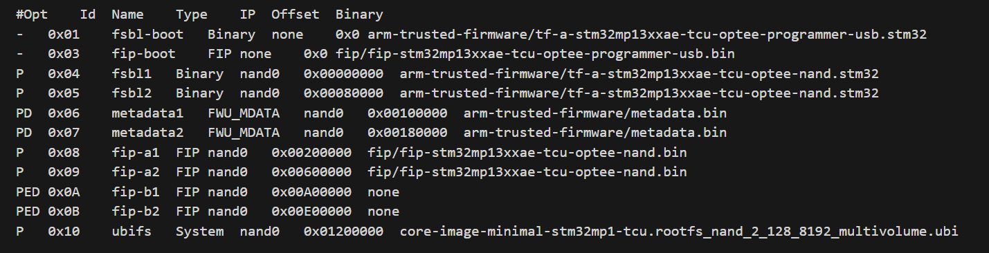
Implementing Fail-safe OTA A/B Updates on STM32MP1
1. Firmware Redundancy (FIP)
2. Configuring OTA A/B with RAUC in Yocto Project
3. Atomic Update Workflow
4. Conclusion
An embedded system not only needs to boot quickly but also must possess robust self-recovery and over-the-air (OTA) update capabilities. Integrating A/B redundancy is the gold standard to ensure the device never becomes “bricked” (unable to boot due to software failure) when an update process unexpectedly fails.
1. Firmware Redundancy (FIP)
Shema of FIP
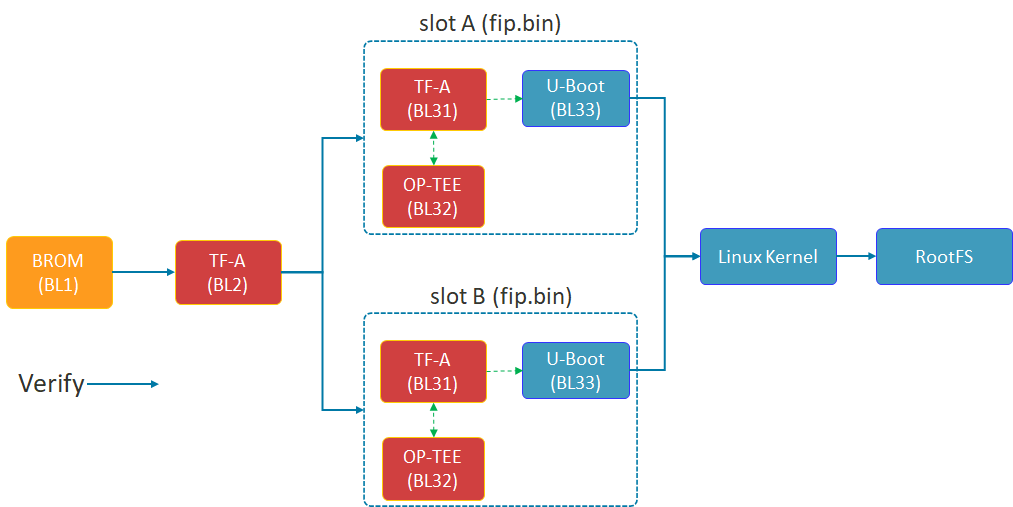
The diagram above illustrates the Chain of Trust (FIP) boot process of the STM32MP1. TF-A (BL2) plays a crucial role in selecting Slot A or Slot B to load the FIP package (including U-Boot and the secure environment) before proceeding to load the Linux Kernel.
The security of the A/B mechanism on the STM32MP1 does not begin with the Linux Kernel, but starts in the very first seconds of the boot process at the lowest Bootloader layer. This is achieved through the FIP (Firmware Image Package) structure.
- TF-A (BL2): This is the first component to run after the ROM code. BL2 acts as the verifying entity. It checks the digital signature and integrity of subsequent partitions. Most importantly, BL2 possesses the logic to choose whether to boot from Slot A or Slot B.
- FIP Container: As shown in the diagram above, each slot (A or B) is an independent fip.bin packet. Inside this container are:
- TF-A (BL31): Manages runtime security services.
- OP-TEE (BL32): Trusted execution environment, protecting sensitive tasks.
- U-Boot (BL33): The main character controlling the Kernel loading process that we optimized for speed in the previous section.
- Fail-over mechanism: If the FIP partition in Slot A fails or doesn’t pass the verification step, BL2 will automatically redirect to Slot B. This is a hardware insurance layer that ensures the device always has a chance to successfully restart.
2. Configuring OTA A/B with RAUC in Yocto Project
Based on the latest documentation from meta-rauc, we will proceed through the following steps:
Step 1: Add the necessary layers.
Open bblayers.conf and add the dependent layers:
Bash
bitbake-layers add-layer layers/meta-rauc
bitbake-layers add-layer layers/meta-openembedded/meta-filesystems
Step 2: Configure Local (local.conf)
Enable RAUC and file system support features:
Code snippet
# Enable RAUC in Distro
DISTRO_FEATURES:append = " rauc"

# Install tools RAUC into Image
IMAGE_INSTALL:append = " rauc u-boot-fw-utils"

# Request Kernel support SquashFS
KERNEL_FEATURES:append = " features/nand/nand-rauc.scc"
Step 3: System Configuration (RAUC-CONF)
Important note from the documentation: Starting with the newer Yocto (Scarthgap) version, configuration files such as system.conf and keyring must be included in a separate recipe called rauc-conf.bb.
Create file recipes-support/rauc/rauc-conf.bbappend in your layer:
Code snippet
FILESEXTRAPATHS:prepend := "${THISDIR}/files:"

# The file system.conf will be auto installed into /etc/rauc/
Step 4: Write the file system.conf for NAND
This file defines the “Slots” so that RAUC understands the partition layout on your device: Ini, TOML
[system]
compatible=stm32mp1-tcu
bootloader=u-boot
statusfile=/var/lib/rauc/status

[slot.rootfs.0]
device=/dev/ubi0_rootfs_a
type=ubifs
bootname=A

[slot.rootfs.1]
device=/dev/ubi0_rootfs_b
type=ubifs
bootname=B
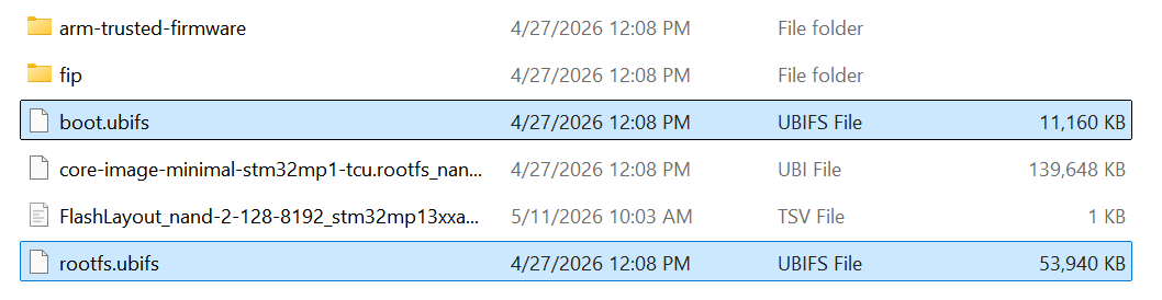
Two files, boot.ubifs and rootfs.ubifs, were created.
3. Atomic Update Workflow
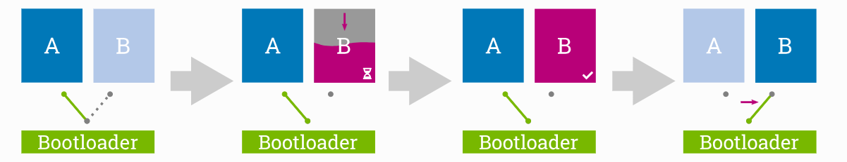
OTA’s 4-STEP PROCESS
The 4-stage update process ensures atomicity: The system only switches the boot region (Switch) to Slot B after the update has been successfully written and fully verified in the background.
The absolute advantage of the A/B Ready mechanism is its atomic update capability. This means the update process is either completely successful and verified, or nothing changes at all — absolutely no in-between state causing system errors.
This process takes place in 4 rigorous stages:
- Stage 1 (Running on A): The system is running normally on Slot A. Slot B acts as an idle memory area (Passive slot), containing an older version of the operating system.
- Stage 2 (Updating B): This is the crucial point for the user experience. The new update is downloaded and written directly to Slot B in the background. The device continues to operate normally, with no downtime during this phase.
- Phase 3 (Verify B): After writing is complete, RAUC performs a digital signature and integrity check. If data is corrupted during transmission, Slot B will be flagged as corrupted, and the system will continue to run safely on Slot A.
- Phase 4 (The Switch): After restarting, the bootloader performs an extremely fast slot switching operation based on optimized environment variables. Thanks to the system streamlining steps in Chapter 2, this “Switch” process is so smooth that users will hardly notice the system has just been upgraded to a completely new version.
4. Conclusion
The successful integration of the OTA A/B Ready mechanism is a crucial step in transforming a prototype into an industry-standard device. In summary, we have achieved:
- Superior performance: Thanks to the strategy of avoiding NAND bandwidth (Lazy Mount) and streamlining Systemd services, the device is no longer bottlenecked during boot-up, providing a smooth instant-on experience.
- High Availability: The A/B mechanism, from the FIP (Firmware) level to the OS (RAUC) level, ensures the device always has a safe exit. If an OTA update fails, the system will automatically fall back to the previous slot, completely eliminating the risk of being “bricked” on-site.
- Future-ready: With the Yocto architecture pre-configured for OTA, maintenance, security patching, and remote feature upgrades are simpler and safer than ever before.
Optimizing boot time is not just a race for numbers, but a matter of reliability. An ideal STM32MP1 system is one that boots up quickly enough to satisfy users, but is also robust enough (A/B Ready) to withstand any update risks. Hopefully, this roadmap from I/O “surgery” to OTA “Bring-up” will help you fully master ST’s powerful MPU line.

Shrinking STM32MP1 Boot Time: Advanced NAND Layout and Lazy Mount Strategies
1. Why Shorten Boot Time?
2. Menthods used to accomplish
2.1. NAND Partition Restructuring & Lazy Mount Strategy for UserFS
2.2. Streamlining Systemd Services (User Space)
2.3. Reducing Log and Console (Bootloader & Kernel)
3. Results Achieved and Overall Assessment
1. Why Shorten Boot Time?
On Linux-based MPUs like the STM32MP1, the default boot time from NAND is often very long, potentially reaching 45 seconds or more. Shortening this time is not just a technical improvement but a mandatory requirement for the following reasons:
- User Experience (UX): In today’s “instant-on” world, users don’t accept having to wait nearly a minute for a handheld device or HMI panel to be ready to operate. Fast boot times create a feeling of robustness and reliability.
- System Responsiveness: For industrial or IoT applications, devices need to be operational and connected as quickly as possible after power is supplied to perform critical tasks such as data collection, actuator configuration control, or alert sending.
- Reliability and Recovery: In the event of a power outage and the system needs to restart (reboot), the shorter the restart time, the less downtime the system experiences, minimizing data risks and maintaining service continuity.
2. Methods used to accomplish
To reduce boot time from approximately 1 minute 10 seconds to under 25 seconds, we need a holistic approach that intervenes in every stage of the boot process (Bootloader → Kernel → Rootfs → User Space).
overall program code structure
Based on the optimization scheme, the core methods applied include:
2.1 NAND Partition Restructuring & Lazy Mount Strategy for UserFS
This change yielded the biggest results. The userfs partition is typically very large (800MB in this example) and contains application data. Having systemd scan and mount this partition at boot time cripples the system due to the slow read speeds of NAND.
The .tsv file was built before modification.
How??
- Flash Layout (TSV): Move the userfs partition to the end of the memory strip, after the critical partitions (bootfs, vendorfs) have been positioned. This optimizes sequential driver reading.
- Configure /etc/fstab (Lazy Mount): Instead of letting the system mount automatically via defaults, reconfigure the userfs mount line using x-systemd.automount.
- Bash
LABEL=userfs /usr/local/user data rw,noauto,x-systemd.automount 0 0
Mechanism: The partition is not mounted during boot. Only when the main application actually accesses /usr/local/user does systemd mount it. This completely frees up this time from the main boot process.
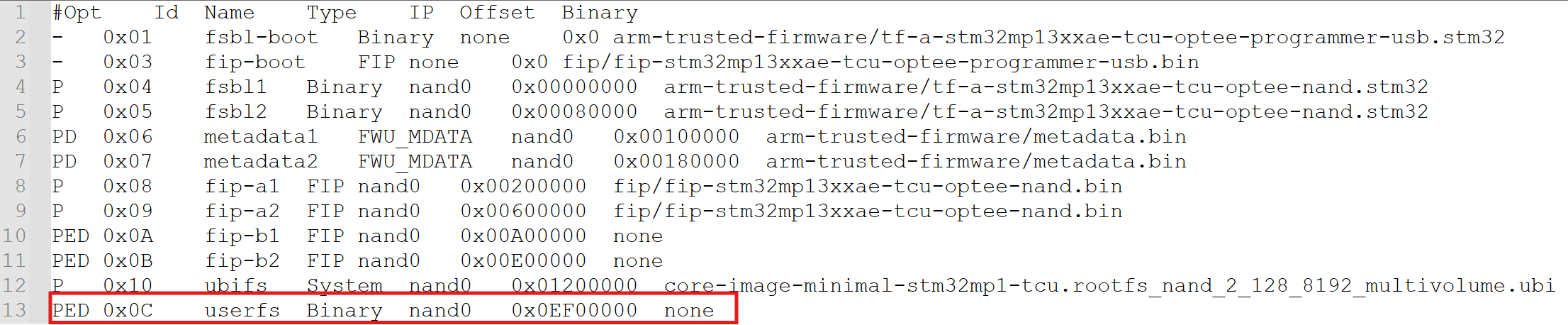
The .tsv file was built after modification.
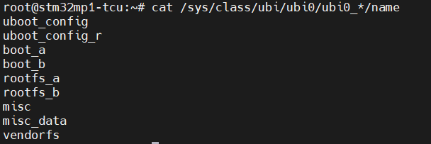
UBI’s logs
Based on the common UBI partition structure on the STM32MP1 (as shown in the device log image, including partitions uboot_config, boot_a, rootfs_a, vendorfs…), we see that the system typically uses a dual-boot (A/B) mechanism to ensure safety during updates. The principle here is to only mount the minimum necessary components to run the kernel and initial user space (such as rootfs and vendorfs). The remaining large data partitions (such as userfs if present, or misc_data) are absolutely not auto-mounted at boot time to avoid clogging the NAND read bandwidth.
2.2 Streamlining Systemd Services (User Space)
The Yocto/OpenSTLinux operating system by default installs many unnecessary services for a “single-app” system (running a single application).
How to do:
Use the `systemctl mask` command to completely disable time-consuming services. We’ll focus on services that are waiting on unused network or hardware:
Bash
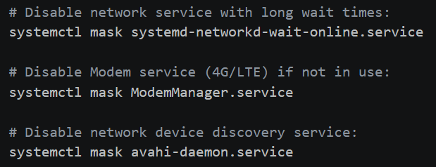
The image below illustrates the specific commands used to “mask” redundant services. In systemd, masking is more powerful than disabling because it links the service to /dev/null, preventing any other service from accidentally triggering it during the boot sequence.
Specific systemctl commands to eliminate boot-time bottlenecks.
2.3 Reducing Log and Console (Bootloader & Kernel)
Printing data to the Serial Console via UART with a low baud rate (115200) is a burden. Each log line represents the CPU’s waiting time for the UART to process.
How to do it:
- U-Boot: Set the key wait time to 0 (setenv bootdelay 0) and (if needed) enable silent mode (setenv silent 1).
- Kernel Command Line (bootargs): Edit the boot configuration file (extlinux.conf) to pass optimal logging parameters to the Kernel.
3. Results Achieved and Overall Assessment
By applying these methods simultaneously, we achieved impressive results. You can see a visual comparison in the “BOOT TIME COMPARISON” chart.
- Initial boot time: Approximately 1 minute 10 seconds.
- Optimized boot time: Reduced to approximately 28 seconds.
- Total time reduction: >30 seconds.
Breakdown time chart showing the reduction in stages (actual on the board):
| Boot Stage | Key Action | Time Reduced |
| Bootloader (U-Boot) | bootdelay=0, disable logs |
1.5s – 2s |
| Linux Kernel Boot | quiet loglevel=3 |
2s – 3s |
| Rootfs/NAND I/O | Delaying & Lazy Mounting UserFS (800MB) | ~20s |
| User Space (Systemd) | systemctl mask <services> |
~5s |
AI-POWERED VIBRATION SENSOR: INTELLIGENCE IN EVERY BEAT
The “Downtime” Nightmare: When the Clock Turns in Dollars

In the fast-paced world of Industry 4.0, every moment of production line downtime is not just the silence of machines, but an uncontrolled “leak” of budget.
- Double damage: You not only lose revenue from reduced production, but also face expensive emergency repair costs and the risk of order delays, eroding your reputation with partners.
- The numbers speak for themselves: According to recent industry reports, the average cost for one hour of unplanned machine downtime can reach tens, even hundreds of thousands of USD depending on the scale.
How to Calculate Your Downtime Costs
To understand why investing in a monitoring system early is crucial, let’s do a practical calculation of what your business actually loses when machinery is down. Before we begin, list the following key parameters:
- Total planned operating time: The number of hours the machine is scheduled to operate (e.g., an 8-hour shift/day).
- Average weekly output: The total number of products the machine produces in a normal week.
- Gross profit per unit: The profit earned for each finished product.
Damage calculation formula
The process for calculating actual damages is established through 3 steps:
- Determine the actual machine downtime: Planned time – Actual running time = Downtime hours
- Calculate the lost productivity:(Total weekly output) / (Planned time) = Production rate per hour
Downtime hours x Rate per hour = Total product shortfall - Determine the total financial damage: Total Product Shortage x Gross Profit/Product = Total Gross Loss
Practical examples
Suppose a piece of equipment on your production line malfunctions and has to be shut down for 3 days.
- Context: The machine operates 8 hours/day (40 hours/week). Average output: 10,000 units/week.
- Efficiency: Production rate is $10,000 / 40 = $250 products/hour.
- Disruption: 3 days of downtime is equivalent to 24 hours of downtime.
| Item | Calculation | Result |
| Lost Production Volume | 24 hours $\times$ 250 units | 6,000 units |
| Financial Damage (Assuming $6 profit/unit) | 6,000 units $\times$ $6 | $36,000 |
The Verdict: In just 3 days of downtime, your business loses $36,000 in gross profit. Note that this figure excludes emergency repair costs, overtime pay for technicians, and potential late-delivery penalties.
This AI-powered solution safeguards your $36,000 investment by detecting anomalies and preventing costly failures before they occur.
Remember: this is just your lost profit. Beyond the expensive professional repairs, the true cost lies in wasted time. It’s time to move past passive monitoring. This solution is more than a measuring device—it’s a revolution in Edge AI. The breakthrough lies in its “brain”: instead of overloading servers with raw data, it analyzes and detects anomalies directly at the source.
- Instantaneous processing: Detects abnormal vibration and temperature readings in milliseconds and issues warnings before problems develop.
- Intelligent data filtering: Only the most important information is transmitted, optimizing network infrastructure and saving operating costs.
- From sensors to experts: With our device, you’re not just installing a device, you’re placing a “24/7 monitoring expert” directly on each machine axis, each “engine”.
Industrial IoT Sensor Node & Rugged Enclosure
Mastering technology: The combination of AI & Qualcomm connectivity
Engineering Research & Development (R&D) Prototype Testing
This solution is more than just a piece of hardware; it is a symbol of the Vietnamese engineering team’s mastery of core technologies. The product represents the culmination of world-leading components and practical, problem-solving thinking tailored for factory environments:
- Edge AI Anomaly Detection – Intelligence at the Edge: The core difference lies in the machine learning algorithms, optimized to run directly on the device’s processor. Instead of passively sending raw data to the Cloud, our solution can “think for itself” and diagnose potential malfunctions on-site. This completely eliminates network latency, ensuring critical alerts are issued instantly before serious incidents occur.
- Qualcomm Super Connectivity – Penetrating All Barriers: In heavy industrial environments where dense metal machinery often causes signal interference, the device fully leverages the strengths of Qualcomm’s antenna technology on its gateway system. The result is ultra-stable connectivity and excellent penetration through obstacles, ensuring a continuous flow of information even in the harshest environments.
Edge AI Controller Board with Qualcomm Connectivity
- Low-power design: This product is the perfect combination of high-end hardware from Analog Devices and the sophisticated programming techniques of our Vietnamese engineering team. By optimizing each processing command and the deep sleep mode of the integrated circuit, the device can operate reliably for many years with only a single battery replacement, helping businesses eliminate concerns regarding regular system maintenance costs.
- Wireless Deployment: With its completely wireless design and intelligent installation structure, our solution redefines the concept of “industrial installation.” There is no need for complex wiring or infrastructure disruption; deploying hundreds of monitoring points across a wide area can be completed in just hours instead of weeks, as required by traditional solutions.
ThingIQ Platform: Optimizing the Orchestration Layer for the Edge AI Ecosystem
If hardware devices act as the Perception (Sensor) and Edge Computing layers, then ThingIQ is the ultimate Orchestration layer. The platform is designed to fully leverage the technical characteristics of strategic hardware partners:
- Physical Layer & Connectivity Management: Leveraging the advantages of Qualcomm chipsets, ThingIQ provides deep monitoring of telecommunications parameters. The system allows flexible configuration of Data Transmission Duty Cycle and Notification Heartbeat, balancing Real-time Latency and Power Consumption based on the signal status at the factory.
- Signal Conditioning: Raw data from power management ICs and sensors of Analog Devices (such as LDO voltage, Fuel-level voltage range) is processed by ThingIQ through standardization algorithms. Users can set Calibration Thresholds directly on the Dashboard to precisely define “Full/Empty” or “Normal/Abnormal Consumption” states, eliminating signal noise before analysis.
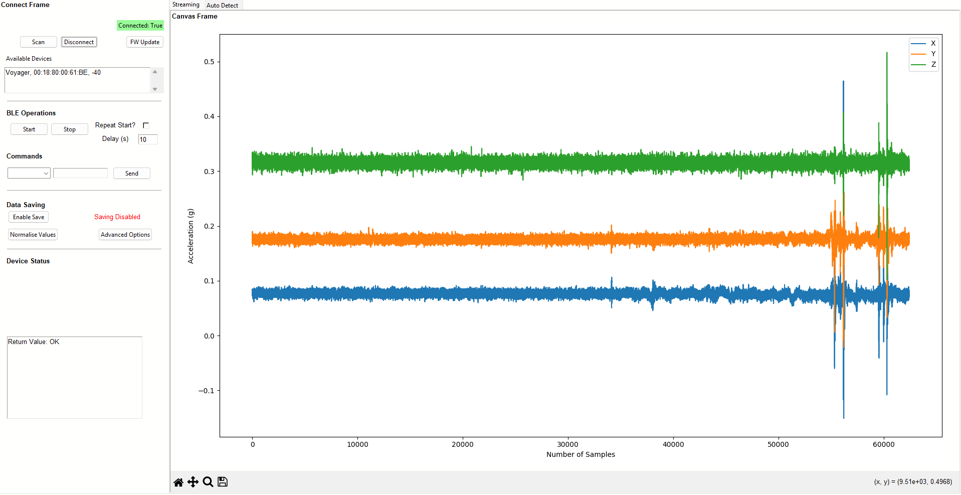
Real-Time Accelerometer Data (X/Y/Z)
- Firmware Operation and Maintenance (FOTA Ecosystem): This is the most important bridge to Edge AI Nodes. ThingIQ manages the entire firmware lifecycle via the FOTA (Firmware Over-The-Air) protocol. With specialized builds (such as version v1.0.3-sf4), administrators can push optimized Inference Models (AI inference models) from the Cloud to edge processors without system disruption. This ensures that Anomaly Detection capabilities are always up-to-date with the latest datasets.
- Massive IoT Management: With a database structure supporting thousands of network nodes (e.g., 1,457 physical records), ThingIQ supports Group Policy Management. Users can group devices by Device Type (Gateway, GPSS, Vibration) or Company/Project to apply consistent configuration profiles, making scaling up the system from a few nodes to thousands of nodes technically feasible and cost-effective.

Contact Us
Don’t let Downtime interrupt your cash flow.
👉 Contact us today for a professional consultation and a live demo at your facility!
Industrial Embedded Solutions Joint Stock Company (IES)
Our mission is to enhance business value by providing effective solutions and professional software applications that meet the rigorous demands of both Vietnamese and international enterprises.
- Hotline 24/7: +84 90 686 2311 | +84 77 413 5678
- Email: [email protected]
- Address: 7A Thoai Ngoc Hau, Hoa Thanh Ward, Tan Phu District, Ho Chi Minh City, Vietnam
- LinkedIn: Industrial Embedded Solutions JSC
Core Services:
- Embedded Systems, Firmware, and Software Development.
- IT Outsourcing & Automotive Technologies.
- Innovative Industrial IoT Solutions.
👉Ready to optimize your operations? Connect with our engineering team now!👈
STM32MP1 NAND Boot Not Working?
Why can’t the STM32MP1 boot from NAND Flash?
1. Layered Boot Chain Mechanism and the Role of ROM Code
1.1. Consistency of STM32 Image Header & Magic Number
1.2. Handshaking Protocol Between FMC and NAND (ONFI Compliance)
1.3. Bad Block Management (BBM) Mechanism
2. Check the Boot Pins (Hardware Strapping) configuration
2.1. Lookup table for Boot Mode STM32MP1.
2.2. How to check the voltage at the BOOT pin[2:0].
3. Compatibility Between ROM Code and ONFI Standard
3.1. How to Determine if a NAND Chip Supports ONFI
3.2. Handling Bus Width Errors (8-bit vs 16-bit) in Hardware
4. File Formatting Errors: The Importance of the STM32 Header
5. Configuring the Device Tree (DTS) for FMC and NAND
5.1. Setting the standard nand-ecc-mode and nand-ecc-strength according to the Datasheet
5.2. Optimizing FMC Clock Speed to Avoid Data Corruption
6. Analyzing Error Codes via UART Console
6.1.Connecting UART4 for ROM Code Debugging
6.2. Decoding Common Boot Failure Hex Codes
7. Checking for Bad Blocks and Flash Layout
7.1. Redundancy of FSBL on NAND
7.2. How to reload Flash Layout using STM32CubeProgrammer via DFU mode
Summary of the Quick Troubleshooting Checklist
Why can’t the STM32MP1 boot from NAND Flash?
To fix the “Silent Boot” error (no console response), we need to delve into the boot chain mechanism of the STM32MP1 system. This process is not simply about reading data; it’s a coordinated sequence between hardware (FMC) and a tightly structured data set defined by the ROM code.
1. Layered Boot Chain Mechanism and the Role of ROM Code
When the system exits the Reset state, the first program to launch is Internal ROM Code. This is immutable source code embedded in the SoC. Its core task is to initialize the FMC (Flexible Memory Controller) to locate and load the FSBL (First Stage Boot Loader) — typically TF-A (Trusted Firmware-A) or U-Boot SPL — into the internal RAM (SYSRAM).
Problems often occur when the authentication chain or data loading process is interrupted at one of the following links:
1.1. Consistency of STM32 Image Header & Magic Number
ROM Code is an extremely strict state machine. It does not execute raw binary files (.bin) because it cannot determine the entry point and data integrity.
- Header Structure (256-byte): Contains important metadata including Image Length, Payload Checksum, and EntryPoint Address (the jump address in SYSRAM).
- Magic Number Identifier: ROM Code scans the blocks to find the code 0x324D5453 (equivalent to the ASCII string “STM3”).
- Consequential Error: If the loaded file is missing this header or the header is offset, ROM Code will return the error “No valid boot device found”. This is why you must use a .stm32 file (processed using mkimage or STM32CubeProgrammer).
1.2. Handshaking Protocol Between FMC and NAND (ONFI Compliance)
Physical layer errors are often caused by incompatibility between the FMC (Flexible Memory Controller) and the memory chip.
- Automatic ONFI detection: The STM32MP1 prioritizes the ONFI (Open NAND Flash Interface) standard for querying operating parameters such as page size, block size, and spare area size. Non-ONFI risk: If the NAND chip does not support ONFI, the ROM code is forced to use default parameters (FMC default timings). If there is a discrepancy in bus width (8-bit vs 16-bit), the read data will be corrupted.
- ECC Mismatch mechanism: This is the “silent killer.” The STM32MP1 uses hardware ECC (BCH4 or BCH8). Configuration error: If the programmer writes data using an ECC algorithm different from the algorithm the ROM Code uses for reading, the checksum will fail and the First Stage Boot Loader (FSBL) will be immediately aborted.
1.3. Bad Block Management (BBM) Mechanism
Unlike stable storage media such as SD Cards or eMMCs, NAND Flash allows for the existence of physical errors (Bad Blocks).
- Redundancy Scan: The ROM Code STM32MP1 will scan at least the first 128 KB to find valid headers.
- Skip-Block Mechanism: When encountering a Factory Bad Block (marked by the manufacturer), the ROM Code will automatically skip it and jump to the next block in the redundancy list.
- Programming Tool Logic Errors: A common technical error is that the programming tool fails to recognize the Bad Block or programs the wrong offset relative to the partition table (Flash Layout). If the FSBL is overwritten on a faulty block without being remapped, the ROM Code will be unable to initialize the Boot Chain.
2. Check the Boot Pins (Hardware Strapping) configuration.
2.1. Lookup table for Boot Mode STM32MP1.
The STM32MP1 boot mode is defined by the combination of several inputs:
- Three boot pins, accessible on ST boards: their possible values are shown in the first column of the table;
- The next column corresponds to the TAMP backup register number 20, that allows the user to force a serial boot when it is set to 0xFF from U-Boot or Linux;
- The one time programmable WORD 3 contains a primary boot source and a secondary boot source, shown in the third and fourth columns, respectively. The possible values for the boot sources are listed in the tables on the right: parallel NAND Flash, QUADSPI NOR Flash, eMMC, SD Card or QUADSPI NAND flash.
The boot pins have two special positions:
- All pins at zero forces a boot in serial mode
- Binary value 100 allows to enter in no boot mode, useful to take the hand on the coprocessor via JTAG for 7 firmware development without Linux.
2.2. How to check the voltage at the BOOT pin[2:0].
Sometimes flipping a switch or soldering resistors doesn’t guarantee the correct logic level due to noise or voltage drop. For accurate debugging, you need to follow these steps:
- Static Voltage Check: Use a multimeter to measure the voltage directly at the test points of the BOOT0, BOOT1, and BOOT2 pins while the board is powered on. High level ≥ 0.7 VDD vs Low level ≤ 0.3 VDD.
- Check for interference (Oscilloscope): The ROM Code only latches the values of the BOOT pins at the rising edge of the NRST signal. If the power supply is slow or the BOOT pin has an excessively large filter capacitor causing delay, the ROM Code may read an incorrect value. Use an oscilloscope to ensure the logic level is stable before releasing NRST.
- Determine the pull-up/pull-down resistance: If you are using resistors to fix logic levels, ensure the resistance value is between 10kΩ and 47kΩ. Avoid using excessively high values (such as 100kΩ) as this can cause logic level deviations due to I/O leakage current.
3. Compatibility Between ROM Code and ONFI Standard
One of the common reasons why the STM32MP1 cannot boot from NAND is the language difference between the ROM code and the flash chip. Unlike older microcontrollers that require hardcoded NAND parameters, the STM32MP1 prioritizes the use of an auto-recognition protocol.
3.1. How to Determine if a NAND Chip Supports ONFI
ONFI (Open NAND Flash Interface) is a standard that allows SoCs to query the technical specifications of NAND chips (such as block count, page size, spare area length) via the 0xEC command.
- Check the datasheet: Search for the keyword “ONFI” in the NAND chip’s technical documentation. Popular chip lines from Micron, Winbond, or Macronix usually support this standard.
- How does the ROM Code handle this?
During boot-up, the ROM Code sends the Read ID (0x90) and Read Parameter Page (0xEC) commands.
If the chip responds with the string “O-N-F-I”, the ROM Code will automatically configure the appropriate FMC controller for that chip.
- If the NAND does not support ONFI (Non-ONFI): The ROM Code will try based on the static ID table (Hardcoded IDs). If your chip is too new or too specific and not on ST’s supported list, the ROM Code won’t know how to read the data, leading to an immediate freeze.
3.2. Handling Bus Width Errors (8-bit vs 16-bit) in Hardware
Discrepancies in data bus width cause Data Mismatch errors, leading the ROM Code to incorrectly read the Bootloader Header.
- STM32MP1 Default: ROM Code initializes the FMC controller in 8-bit mode for backward compatibility.
- Using 16-bit NAND: If you are using a 16-bit NAND chip, the FMC_NIORDY pin (or some specific pin configuration) must be handled correctly. Most importantly, the STM32MP1 ROM Code only supports booting from 8-bit NAND. If your hardware design uses a 16-bit bus for the Boot partition, the system will not be able to boot (unless the NAND chip has an automatic 8-bit switching mode upon receiving a command).
- Physical connection check: Ensure that the signal lines from FMC_D0 to FMC_D7 are not short-circuited or open-circuited. Transmission impedance: With high access speeds, the data bus lines need to be of similar length to avoid signal skew.
4. File Formatting Errors: The Importance of the STM32 Header
A common mistake made by engineers new to the STM32MP1 family is directly loading raw binary files (.bin) onto NAND Flash. In reality, the STM32MP1’s ROM code doesn’t automatically understand where the binary file starts. It requires a technical “wrapper” surrounding the actual data, called the STM32 Image Header. If the loaded file lacks this header, the system will treat it as garbage and completely ignore it.
What is Magic Number 0x324D5453 Structure?
Each boot file (TF-A, U-Boot SPL) loaded onto NAND must begin with a 256-byte header. The most important component in this header is the Magic Number.
- Value: 0x324D5453 (When read in Little-endian format, it corresponds to the ASCII character string: “S-T-M-3”).
- Role: This is the “key” to unlock the ROM Code. When scanning through the Blocks on the NAND, the ROM Code only searches for this number. If the first 4 bytes of the Block do not match 0x324D5453, the ROM Code will immediately jump to the next Block.
- Other components in the Header: Image Signature, Image Length, Entry Point
When you compile with Yocto or Buildroot, the script will call the mkimage tool to package the u-boot-spl.bin file into u-boot-spl.stm32. This .stm32 extension is the indicator that the Header has been inserted. Otherwise you can use STM32CubeProgrammer to check Header:
- You can open the .stm32 file using Hex Editor software (such as HxD). If you see the first 4 bytes as 53 4D 54 32 (corresponding to “STM3”), your file has a standard header.
- When you connect the board in USB DFU mode, load the file into the corresponding partition: If you select a file without a header, the tool will immediately warn of a formatting error or the boot process will fail with the error log: “Header Not Found”. Using Flash Layout: The .tsv (Flash Layout) file in STM32CubeProgrammer will define partitions such as fsbl1, fsbl2. This tool automatically checks the integrity of the header before pushing data to the NAND.
5. Configuring the Device Tree (DTS) for FMC and NAND
After the ROM Code has successfully loaded the FSBL, the next stage (U-Boot and Kernel) depends entirely on the data structure in the Device Tree (.dts). If the parameters here do not match the physical characteristics of the NAND chip, the system will freeze when trying to mount the data partition or report an “ECC uncorrectable error”.
5.1. Setting the standard nand-ecc-mode and nand-ecc-strength according to the Datasheet
To ensure data integrity, you need to open the datasheet of your NAND chip and find the “ECC Requirement” section.
- nand-ecc-mode: For STM32MP1, this value is usually “hw” (using hardware FMC acceleration). If your NAND chip has built-in error correction, use “on-die”.
- nand-ecc-strength: The number of error bits the controller is capable of correcting per data area (Step size).
Example: If the datasheet requires “8-bit ECC per 512 bytes”, set nand-ecc-strength = <8>. Note: STM32MP1 supports different strength levels (BCH4, BCH8). If the NAND chip requires 8-bit and you only configure 4-bit, the system will run unstably and quickly suffer from file corruption.
5.2. Optimizing FMC Clock Speed to Avoid Data Corruption
Excessively high FMC control clock speeds cause random bit flips. The FMC controller must be configured with timings that match the NAND chip’s access speed.
- EBI Timings: Parameters such as tset, twait, and hold in the Device Tree define the minimum time for the data signal to stabilize before processing by the chip.
- Check Clock Speed: If you see many unidentified read errors in the U-Boot log, try reducing the FMC bus clock speed by adjusting it in the st,fmc-control button or reconfiguring the Clock Tree in the system’s .dts file.
6. Analyzing Error Codes via UART Console
When your STM32MP1 remains silent, the Internal ROM Code provides a “last-resort” diagnostic tool. Even before the first line of your code executes, the ROM Code can output specific error status characters to help you pinpoint exactly where the boot process failed.
6.1.Connecting UART4 for ROM Code Debugging
In STMicroelectronics reference designs (such as the Discovery or Eval boards), UART4 is the dedicated default console for ROM Code and bootloader debugging.
Default Pin Assignment:
- UART4_TX: Pin PG11 (Usually routed through an onboard ST-LINK or USB-to-UART bridge).
- UART4_RX: Pin PB2.
Terminal Configuration:
- Baud rate: 115200
- Data bits: 8
- Parity: None
- Stop bits: 1
- Flow Control: None
6.2. Decoding Common Boot Failure Hex Codes
If the NAND boot fails, the ROM Code emits an error character as defined in the AN5031 technical application note. Below is a breakdown of the most common codes encountered during NAND debugging:
| Hex Code | Technical Meaning (Error Meaning) | Troubleshooting / Solution |
|---|---|---|
| 0x61 | No Valid Header Found | The ROM Code scanned the entire NAND but did not find the Magic Number 0x324D5453. Check the .stm32 header file again. |
| 0x62 | Invalid Image Checksum | The header was found, but the internal data is corrupted or the ECC does not match. Verify the ECC configuration used during flashing. |
| 0x63 | Device Timeout / Not Ready | The NAND chip does not respond to read commands. Check the power supply (1.8V/3.3V) and the Ready/Busy (R/B) pin. |
| 0x64 | NAND ID Not Supported | The ROM Code can read the chip ID but does not support it (usually because it is not ONFI compliant). |
| 0x65 | Authentication Failed | This occurs when Secure Boot is enabled but the digital signature is invalid. |
7. Checking for Bad Blocks and Flash Layout
Unlike other memory types such as eMMC or SD Card, NAND Flash always comes with faulty blocks (bad blocks) from the factory. If the FSBL (TF-A) accidentally lands on a bad block without a redundancy mechanism, the STM32MP1 will never boot.
7.1. Redundancy of FSBL on NAND
The ROM code of the STM32MP1 is extremely intelligently designed to deal with bad blocks through a redundancy mechanism.
- FSBL Mirroring: Typically, we don’t just load a single FSBL. The system usually requires at least 2 to 5 copies of the FSBL (denoted as fsbl1, fsbl2, fsbl3…) located in the first blocks of the NAND.
- ROM Code Scanning Mechanism: 1. ROM Code starts scanning from Block 0. 2. If Block 0 is corrupted or lacks a valid STM32 header, it automatically jumps to the next block (usually Block 1 or the next offset depending on the configuration). 3. This process repeats until a complete FSBL is found.
- Offset Location: Typically, FSBLs are located at fixed positions (e.g., 0x00000000, 0x00040000, 0x00080000…). If you only load an fsbl1 into Block 0 and that block fails, the system will freeze.
7.2. How to reload Flash Layout using STM32CubeProgrammer via DFU mode
When NAND boot fails completely, the most thorough solution is to reload the entire partition structure via USB DFU (Device Firmware Update) mode.
Step 1: Firstly, switch to Serial Boot mode
Set the BOOT pins to level 000 (as instructed in section 1) and connect the board to the computer via USB OTG port.
Step 2: Next, prepare the Flash Layout file (.tsv)
The .tsv file is a “map” defining the location of each component on the NAND. A standard NAND file usually looks like this:
Note: The Offset column must match the Erase Size architecture of the NAND chip you are using.
Step 3: Finally, flashing the file
- Open STM32CubeProgrammer.
- Select the USB connection and click Connect.
- Switch to the Erasing & Programming tab and select the prepared .tsv file.
- Click Download.
- The tool will automatically remove bad blocks, calculate ECC values, and flash headers for each partition.
- If you encounter a Partition overlap error, check the file size against the offset.
Summary of the Quick Troubleshooting Checklist
| Category | Checklist Item | Status | Technical Notes |
|---|---|---|---|
| 1. Hardware | Boot Pins Strapping | [ ] | Ensure BOOT[2:0] = 010 (NAND Boot mode). |
| Voltage Levels | [ ] | Measure BOOT pins: High ≥ 0.7 VDD, Low ≤ 0.3 VDD. | |
| Bus Width | [ ] | ROM Code supports 8-bit NAND by default. | |
| Ready/Busy (R/B) | [ ] | Check pull-up resistor and connection to the SoC. | |
| 2. Image Header | Magic Number | [ ] | The first 4 bytes of the file must be 53 4D 54 32 (“STM3”). |
| File Extension | [ ] | Use .stm32 file, not a raw .bin file. | |
| Entry Point | [ ] | Must match the mapped address in SYSRAM. | |
| 3. NAND & ECC | ONFI Support | [ ] | Confirm the NAND supports ONFI or is in ST’s supported list. |
| ECC Strength | [ ] | Match nand-ecc-strength in DTS with the datasheet (4-bit / 8-bit). | |
| ECC Mode | [ ] | If using On-die ECC, disable FMC Hardware ECC. | |
| 4. Software / DTS | FSBL Redundancy | [ ] | Flash at least two copies (fsbl1, fsbl2) at the correct offsets. |
| TSV Partition | [ ] | Check the .tsv file to ensure no partition overlap. | |
| FMC Timings | [ ] | Increase tset and twait in DTS if random data errors occur. | |
| 5. Diagnostics | UART4 Log | [ ] | 115200, 8N1. Check Hex error codes (0x61, 0x62, 0x63). |
| USB DFU Mode | [ ] | Set BOOT to 000 to test connection via STM32CubeProg. |
📞 Technical Support & Consulting
Struggling with complex timing issues or custom hardware integration? We are here to help you accelerate your time-to-market.
Contact our embedded engineers at IES (Industrial Embedded Solutions) with email address [email protected] for expert hardware design review, custom bootloader development, and Linux kernel optimization.
STM32MP1 Custom Board Bring-Up and Flashing Procedure
Bring-up Board STM32MP1
1. Bring-up steps
2. DDR Tuning & Stress Test
The Flashing Chain
Check Verify Issue
Bring-up Board STM32MP1
1. Bring-up steps
Step 1: Check the hardware baseline.
Before powering on, ensure that the basic physical parameters do not cause a short circuit.
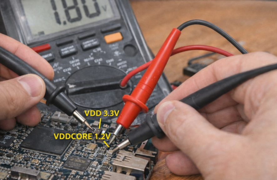
- Check the power supply: Use a multimeter (VOM) to measure the impedance of the main power lines (V_DDCORE, V_DD\_DDR, V_DD).
- Power on: Observe the board’s current consumption. If the current spikes (High current), disconnect the power immediately.
- Check the PMIC: Measure the output voltage at the capacitors surrounding the PMIC (STPMIC1). Ensure the voltage is 1.2V for the Core and 1.35V or 1.5V for the DDR.
Step 2: Set up Boot Pins (Boot Configuration)
1. Principles of Interfering with BootROM Logic
Each microprocessor, upon leaving the factory, has a fixed, unchangeable piece of code called BootROM. When power is applied, BootROM scans the voltage state (Logic High/Low) on dedicated configuration pins such as BOOT0, BOOT1, and BOOT2.
- Mechanism: Flipping the switches (DIP switches) or changing the pull-up/pull-down resistors sends an “encoding signal” to the microprocessor.
- Purpose: To instruct the chip to skip searching for software in the internal storage memory (which is usually empty) and go straight to waiting for commands from external communication ports.
2. USB OTG Priority Mode (DFU Mode)
For the STM32MP1 series, the binary configuration is usually set to 000 (or according to the manufacturer’s specific reference diagram) to prioritize USB OTG (Device) mode.
- DFU (Device Firmware Upgrade): In this mode, the processor acts as a slave device. As soon as it connects to the Host PC via a USB Type-C cable, the BootROM will initialize a minimal USB stack so that the computer can recognize the device as a “USB DFU Device”. This is the state that allows the STM32CubeProgrammer tool to “see” the chip and be ready to transfer data.
3. Physical Bring-up Chain Diagram
To ensure stable and reliable data transmission, the bring-up chain diagram must adhere to the following structure:
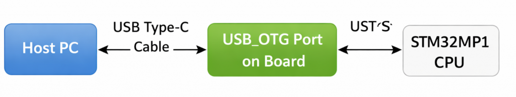
In this connection chain, the USB_OTG port acts as the sole gateway. Correctly configuring the BOOT pins “opens” this gateway, allowing data from the computer to go directly to the lowest hardware layer of the CPU without passing through any running operating system.
Step 3: Check the connection with the Host PC (DFU Mode)
When you connect the device to the computer and select the USB interface in the STM32CubeProgrammer tool, a digital “handshake” process takes place. If the BOOT pin configuration in the previous step was correct, the chip’s BootROM will send identification parameters (Vendor ID and Product ID) to the computer. When you press Connect, the software will query the chip’s unique Serial Number and display the “Connected” status.
Technical Significance of a Successful Connection
A stable connection is practical proof that the Minimum Operating Conditions have been met:
- CPU “Live”: The main logic block of the microprocessor is active and executing code from the BootROM.
- Power System (PMIC/LDO): The core power lines (VDD, VDDCORE, VDD_USB) are providing stable voltage, without voltage drops or interference.
- Oscillator (Clocking): The quartz crystal (usually 24MHz) is oscillating accurately, allowing the frequency multiplier (PLL) inside the chip to generate the necessary clock pulse for the USB controller.
Analyzing the Cause of Connection Failure
If the computer reports “USB Device Not Recognized” or the device is not found, this is a warning signal of a physical error on the hardware layer:
- Clock Error: If the 24MHz quartz crystal is not working or is at the wrong frequency, the USB controller will be unable to synchronize data with the Host PC, resulting in the device being “invisible” to the software.
- Signal Integrity: The USB D+/D- differential signal pair needs to be checked. Even a small design flaw (such as unbalanced 90 Ohm impedance) or a mechanical contact error will interrupt the data flow.
- Boot Status: The CPU may still be stuck in Flash boot mode instead of entering Load Mode (DFU), requiring a check of the logic levels on the BOOT0/1/2 pins.
2. DDR Tuning & Stress Test
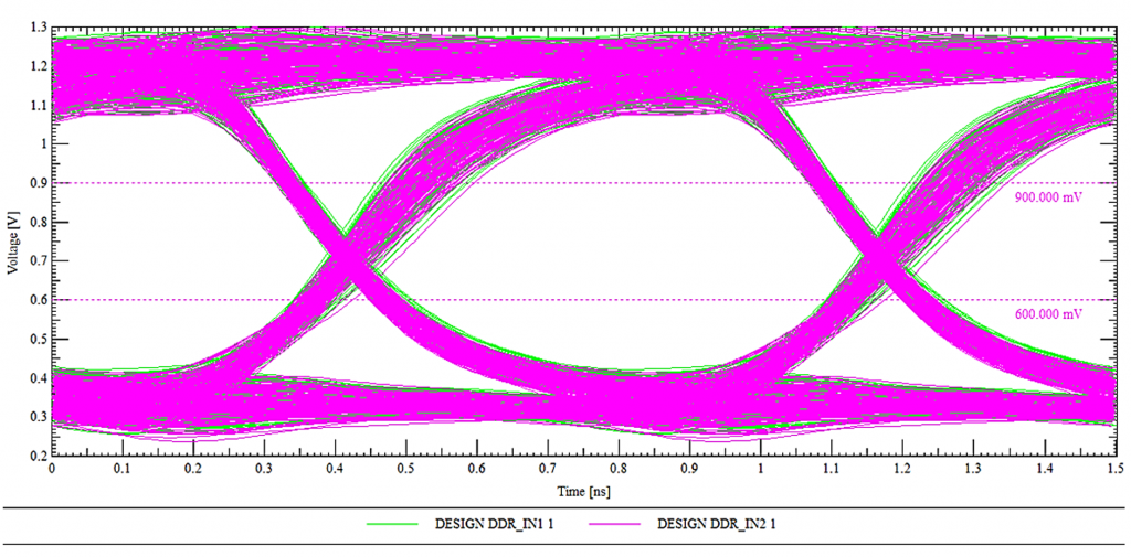
Eye Diagram for DDR
During the DDR bring-up process, simply checking if the RAM is fully recognized isn’t enough. We need to observe the Eye Diagram.
- If the ‘eye’ is wide and clean: The signal is extremely stable, the Timing and Voltage Swing parameters are optimized, and the system will run reliably 24/7 without crashing.
- If the ‘eye’ is narrow or noisy (Closed eye): This means the PCB traces are too long, there’s crosstalk, or the Drive Strength configuration is incorrect. This is the cause of random kernel panics that are very difficult to debug later.
The image above shows an Eye Diagram of a DDR signal, created by overlaying multiple signal cycles in the time domain. The horizontal axis represents time (ns), while the vertical axis represents voltage (V), allowing for simultaneous evaluation of the signal’s timing and amplitude characteristics. The “eye opening” represents the time and voltage range at which data can be safely sampled. A clear, wide eye indicates a signal with low noise, small jitter, and good timing margin, thus ensuring stable high-speed data transmission on the DDR bus. The pink and green signal lines represent multiple samples of different data bits, overlaid to reflect the actual signal variation. The reference voltage level lines (e.g., ~0.6V and ~0.9V) serve as logical thresholds, helping to determine the ability to distinguish between ‘0’ and ‘1’ levels. This diagram is a crucial tool in the bring-up and optimization process, especially when evaluating DDR signal quality. A properly calibrated Eye Diagram is essential to ensuring accurate and reliable DDR initialization and data transfer.
After the computer recognizes the chip, the next step in bring-up is to get the RAM working. If the RAM is faulty, you will never be able to boot Linux.
- Tool: Use the DDR Tool tab in STM32CubeMX.
- Procedure:
- Load the RAM configuration file (DDR3/LPDDR3) into the tool.
- Click Test: The tool will load a small piece of code into the SRAM to test the read/write capabilities of the external RAM
- DDR Training: The system automatically calculates the latency (skew) of the signal lines on the PCB to provide the optimal set of parameters.
The Flashing Chain
Because the SRAM of the STM32MP1 is very small, we cannot directly load an image file of several hundred MB into Flash memory. The process must be done in a “bridging” fashion: loading the small programmer to power the larger programmer, and then loading the actual data.
Step 1: Prepare the FlashLayout file (.tsv)
The configuration file (usually a Flash Layout) acts as the orchestrator of the entire system loading process, establishing key operating parameters for the loading tool. First, this file configures the physical layer by defining the connection protocol (USB/UART) to establish data flow between the Host PC and the Target. The core of the file is the Partition Map, which details the ID identifiers, system partition names (such as ssbl, boot, rootfs), and addresses mapped from executable files (.stm32, .bin) on the computer to the target memory.
A standard partition structure is established in a hierarchical logical sequence to ensure a reliable boot sequence: starting with the FSBL (TF-A) responsible for low-level hardware initialization, followed by the SSBL (U-Boot) acting as the second-stage loader, then the Boot Partition (containing the Kernel and DTB), and finally the RootFS (User Space) storage space. By tightly managing these indices, the flashing process ensures data integrity and consistency in the partition structure on the storage device.

Step 2: Load the primer phase (DFU phase)
In the architecture of application-oriented microprocessors like the STM32MP1, when the system has no software in its internal memory (eMMC/SD), it enters a state of “empty” control resources. The Primer phase is a crucial intermediate step to establish the execution environment in RAM before data can be written to Flash.
1. Loading TF-A (FSBL) into Internal SRAM: Initializing the Physical Layer
When the “Download” command is triggered from the STM32CubeProgrammer, the first process is to push the TF-A (Trusted Firmware-A) file, the version supporting the USB protocol, into the Internal SRAM.
- Principle: Because at boot time, the external DDR RAM is not yet configured and cannot be used, the system is forced to utilize the SRAM integrated within the chip (limited capacity but available power and instantaneous access).
- Key Task: As soon as it’s loaded into SRAM, the TF-A performs the most important task: configuring the DDR RAM controller and setting the voltage and clock speed parameters for the external RAM module. This is the “opening step” to provide the system with sufficient temporary storage space for the subsequent steps.
2. Loading U-Boot (SSBL) into DDR RAM: Setting up the storage controller
After the TF-A confirms the DDR RAM is ready for operation, the computer pushes the U-Boot file (usually in .stm32 format) into this DDR RAM memory.
- Principle: Unlike the TF-A, which focuses only on low-level hardware initialization, the U-Boot is a second-stage loader (SSBL) with a rich driver system.
- Key task: When U-Boot is executed from DDR RAM, it activates more complex communication protocols such as SDMMC (for SD/eMMC cards) or QSPI. At this point, the processor officially becomes capable of “understanding” and “communicating” with Flash memory.
3. The Role of the DFU “Bridge”
At the end of the Primer Phase, the device has transformed from a rudimentary hardware block into a system with full resource control:
- SRAM acts as the bootstrap.
- DDR RAM acts as a large-capacity data buffer.
- U-Boot acts as the “manager,” executing write commands directly from the USB data stream to the blocks on the eMMC/SD Card.
When you click “Download” on STM32CubeProgrammer:
- Load TF-A into SRAM: The USB version of the TF-A file is pushed into SRAM. The chip starts running TF-A to initialize DDR RAM.
- Load U-Boot into DDR: After the RAM is loaded, the computer pushes the U-Boot file (usually u-boot-stm32mp1…stm32) into DDR. At this point, U-Boot takes control and activates the eMMC/SD Card drivers.
Step 3: Write the data to storage memory.
U-Boot will open a “channel” to receive data from the computer via USB and write it directly to the partitions on the eMMC/SD Card according to the scheme in the .tsv file.
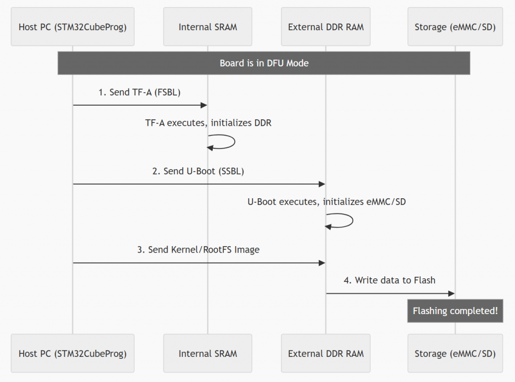
Flashing Process Diagram (Sequence Diagram)
The process shown in the image illustrates the flashing steps for an embedded system (typically the STM32MP1 series) via DFU (Device Firmware Upgrade) mode. This process is performed using a step-by-step “priming” mechanism to gradually initialize complex hardware components.
First, when the device is in DFU mode, the host PC sends the first-stage bootloader (TF-A/FSBL) to the internal SRAM. After the TF-A executes and activates the external DDR RAM, the PC continues to send the second-stage bootloader (U-Boot/SSBL) to it. At this point, U-Boot acts as a controller to initiate communication with storage devices such as eMMC or SD cards. Finally, larger operating system files (such as Kernel or RootFS) are loaded into DDR RAM and then officially written to Flash memory. The process ends when all data has been successfully loaded into permanent storage, allowing the device to boot up independently afterward.
Check verify issue
The golden rule: “The earlier the error appears, the closer the problem is to the hardware.” We will divide this into four main bottlenecks corresponding to the four boot stages.
- Issue 1: No Boot Log
- Issue 2: Freezes at FSBL (DDR/RAM Error)
- Issue 3: Hanging at SSBL (Storage/MMC Error)
- Issue 4: Kernel Panic (Linux Kernel & RootFS Error)
The systematization of the Bring-up process is not just a set of individual tests, but a logical process that strictly adheres to the Hardware Boot Chain. The core principle is hierarchical diagnostics: validating minimum operating conditions at the low level before expanding to more complex peripherals.
Each issue analyzed, from the silence of the No Boot Log to the crash of the Kernel Panic, marks a specific stop point (hang) in the boot process. To visualize the diagnostic priority order and how these issues are distributed across architectural layers, the diagnostic diagram below provides an overview of the boot event sequence.
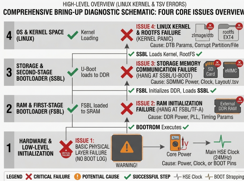
The diagram above clearly establishes a hierarchical diagnostic structure, progressing from the lowest Hardware & Low-level layer to the highest OS & Kernel Space layer. Red X marks indicate failed execution stages triggered by specific potential causes, while green checkmarks confirm successful execution steps.
This diagram serves as a quick diagnostic tool to pinpoint the problematic architecture layer. However, to transition from identifying errors (e.g., Treo at the Storage layer) to implementing specific technical solutions, a detailed action checklist is needed. The summary table below systematizes this visual diagram into a technical checklist, defining the components to be checked, the necessary tools, and specific implementation solutions for each error layer.
| Priority | Issue | Symptom Description | Component to Check | Checking Tool/Method | Specific Solution |
| 1 | Issue 1: Basic Physical Layer Failure (No Boot Log) | Board is completely silent. UART does not log. PC does not recognize USB DFU. |
1. Power Tree.
2. Clocking (24MHz HSE).
3. BOOT Configuration Pins (BOOT[2:0]). |
– Multimeter.
– Oscilloscope.
– Observe Switches/Resistors. |
– Measure VDDCORE, VDD_DDR, VDD.
– Measure crystal waveform.
– Set BOOT Switches to 000 (DFU). |
| 2 | Issue 2: RAM Initialization Failure (Hang at FSBL/TF-A) | Initial logs appear (BootROM/FSBL), then hangs completely. Last log is typically ‘DDR Initialization’. |
1. DDR PHY VDD (Power for RAM physical layer).
2. DDR Clock Tree (PLL_DDR).
3. DDR Parameters (Layout TSV / Device Tree |
– Multimeter (measure voltage drop).
– Refer to documentation (Datasheet, Schematic).
– TSV configuration file. |
– Check for stable VDD_DDR power.
– Check PLL_DDR in DTB.
– Compare DDR Timing Params with the RAM chip datasheet. |
| 3 | Issue 3: Storage Memory Communication Failure (Hang at SSBL/U-Boot) | U-Boot runs successfully, recognizes RAM, but hangs when attempting to access SD/eMMC. Last log is ‘Mounting’ or ‘Failed to read partition’. |
1. SDMMC VDD/VCC (Power for SD card/eMMC).
2. SDMMC Clock Tree.
3. Driver Configuration (U-Boot DTB / Flash Layout |
– Multimeter.
– Check TSV file for partition location.
– Check U-Boot Device Tree |
– Ensure SDMMC power is operational.
– Check
– Validate partition ID/address in the |
| 4 | Issue 4: Linux Kernel & RootFS Failure (Kernel Panic) | U-Boot successfully loads Kernel/DTB. Kernel begins to run, then crashes (Panic). Console displays ‘Kernel Panic’, ‘VFS: Unable to mount root fs’. |
1. Kernel Image Integrity (Data Corruption).
2. Kernel DTB Configuration (Incorrect DTB parameters).
3. RootFS Integrity (RootFS partition corruption). |
– Checksum (MD5/SHA).
– Look up
– Check EXT4 format of the RootFS. |
– Verify checksum of Kernel/RootFS files.
– Modify
– Attempt to recreate the RootFS partition ( |
STM32MP1 Bootchain: From BootROM to Linux
In embedded systems running Linux, the boot process is not simply a matter of turning on the power and running the operating system. Especially with the STM32MP1 processor family, the bootchain is designed as a multi-stage boot to ensure flexibility, security, and the ability to configure complex hardware.
From the moment power is applied, the system goes through a series of consecutive steps: from the internal BootROM, to a low-level bootloader like Trusted Firmware-A, followed by a high-level bootloader like U-Boot, and finally to the Linux kernel and user space. Each stage has its own role and is closely interdependent.
Understanding the bootchain is not only crucial for grasping how the system boots, but it’s also key to:
- Debug boot errors (TF-A freezes, DDR errors, kernel panics, etc.)
- Customize the system as needed (change boot mode, optimize boot time)
- Develop and integrate firmware efficiently
In this article, we will delve into each stage of the bootchain on the STM32MP1, accompanied by illustrative diagrams and detailed analysis so you can understand the entire process from power-up to Linux being ready to operate.
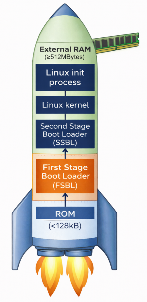
Why does the STM32MP1 need multi-stage boot?
Unlike simpler microcontrollers, the STM32MP1 is a complex multi-processor unit (MPU). It requires multi-stage boot for two core reasons. First, there’s the limitation of internal memory; upon power-on, the system only has a small amount of internal SRAM (less than 256KB). This is insufficient to accommodate the entire Linux Kernel (which weighs tens of MB); therefore, intermediate steps are needed to “wake up” external RAM (DDR). Second, flexibility and security are important. Breaking down the stages allows developers to customize hardware configurations (such as RAM type and storage devices) and establish security layers (Secure Boot) before the operating system officially takes control.
Overview of the main stages:
- BootROM: Internal source code responsible for finding the first boot device.
- FSBL (First Stage Bootloader): Usually TF-A, its main task is to configure DDR RAM and set up a secure environment.
- SSBL (Second Stage Bootloader): Usually U-Boot, provides file management features and prepares the kernel loading environment.
- Linux Kernel: The heart of the operating system, managing resources and controlling peripheral devices.
- RootFS: The file system containing applications, libraries, and the end-user interface.
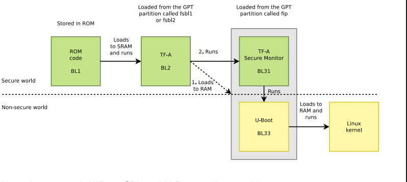
ROM Code

The ROM code in the STM32MP1 is immutable, meaning it cannot be changed, deleted, or overwritten by the user, thus acting as the most reliable software in the entire system. Immediately after the reset signal is released, the ROM code begins execution almost instantaneously, ensuring a fast and stable boot process. Importantly, it operates in a very limited environment – when the system has no external RAM, no high clock speed, and relies solely on the chip’s internal oscillator and SRAM to perform initial tasks.
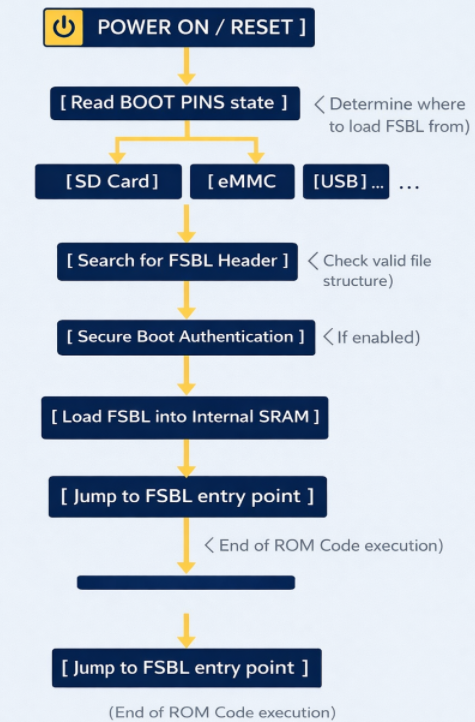
ROM Code schematic diagram
The ROM code checks the physical state (high/low) of the dedicated pins on the chip. Based on this, it knows where to find the FSBL file (SD Card, eMMC, NAND/NOR Flash, USB (DFU Mode), etc.). To read data from an SD Card or USB, the ROM code contains extremely rudimentary drivers for the SDMMC, SPI, or USB controllers. It doesn’t need an operating system; it communicates directly with the hardware at the lowest level.
The ROM code searches for a special data structure called the STM32 Header in the first bytes of external memory. This header contains information about the file size and destination address in SRAM.
If Secure Boot mode is enabled, the ROM code uses encryption algorithms (such as ECDSA) to verify the digital signature of the FSBL. If the file has been illegally modified, the chip will refuse to boot to protect the system.
After everything is valid, the ROM Code copies the entire FSBL (TF-A) file to the Internal SRAM. Then, it executes a jump instruction (Branch) to the starting address of the FSBL. From this moment on, the ROM Code “retreats” and does not participate in the operation until the next Reset.
First Stage Boot Loader (FSBL)
TF-A is an industry standard from ARM. It was chosen as the FSBL for the STM32MP1 because of its robust security handling capabilities and the ability to perform hardware-intensive initialization that conventional bootloaders struggle to achieve within the limited memory space of SRAM.
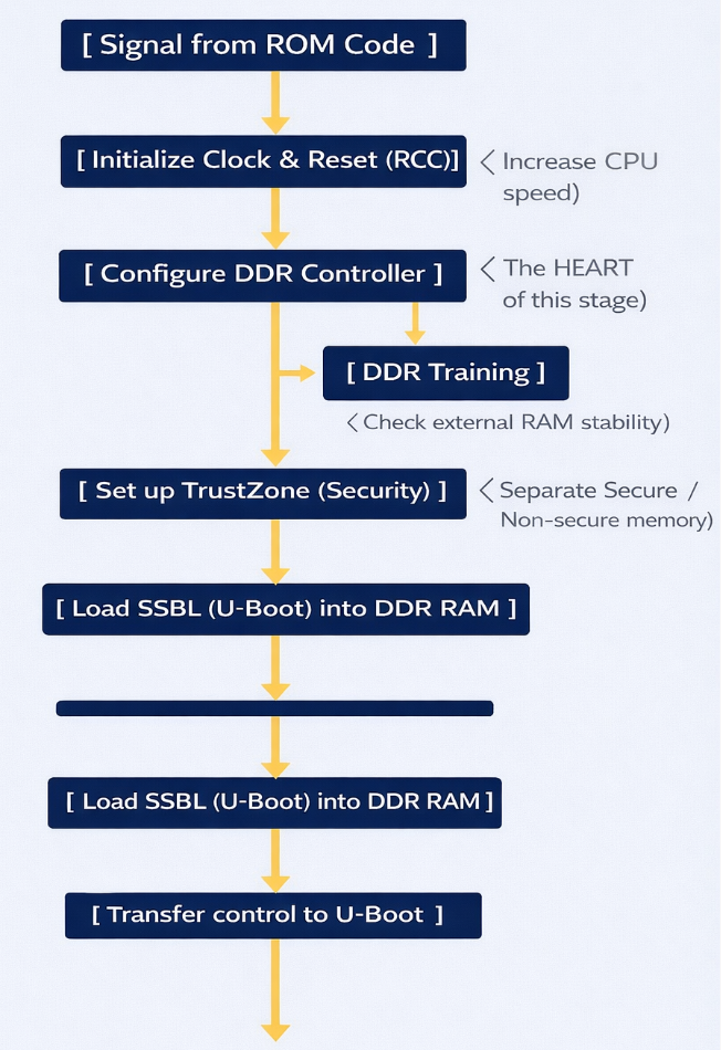
FSBL Schematic diagram
Task: (DDR Initialization) – This is the most important task. The DDR controller is an extremely complex hardware unit. The FSBL must:
- Set precise timing parameters down to the nanosecond for the type of RAM being used (DDR3, LPDDR3, etc.).
- Perform DDR Training: Send test data strings to align the signal between the chip and RAM, ensuring that data is not corrupted during high-speed transmission.
- Result: After this step, the system, which initially had only ~256KB of SRAM, can now access 512MB – 1GB of DDR RAM.
ROM Code runs at very low speeds. The FSBL will configure the power multipliers (PLLs) to push the CPU clock speed higher, allowing for faster operating system loading. It also sets up the voltage regulators (PMICs) to provide stable power to other components.
The STM32MP1 uses TrustZone technology. The FSBL is responsible for clearly defining:
- Secure World: Where sensitive tasks (encryption, digital signatures) run.
- Normal World: Where Linux and user applications run. It establishes separations to prevent Linux from illegally interfering with secure memory areas.
The FSBL runs entirely within internal SRAM. Because this space is very small, TF-A is designed in smaller “stages” like BL2. It has no user interface; you only see short logs via the serial port indicating whether the DDR initialization process was successful or failed.
Second Stage Boot Loader (SSBL)
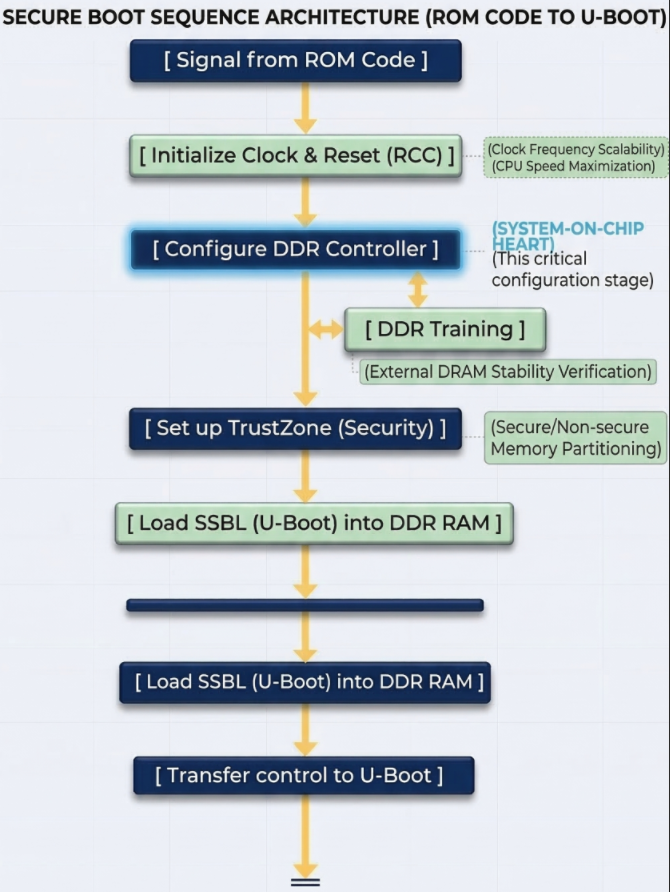
U-Boot’s core functions:
- File System Management: This is U-Boot’s strongest point. It has drivers to understand partition formats like FAT32 or EXT4. This allows it to find the correct uImage or zImage file located deep within the memory card’s directories and load it into RAM.
- Device Tree (DTB) Usage: U-Boot not only loads the Kernel but also the Device Tree file. This is a map describing the hardware (which pins are for LEDs, which are for I2C, etc.). U-Boot can edit this map “on the fly” (while running) before delivering it to Linux, making the system more flexible.;
- Interactive Environment (U-Boot Shell): This is the only stage in the Bootchain where humans can intervene.
U-Boot on the STM32MP1 is usually stored in a separate partition (often named ssbl). If you want to change the boot logo or change the boot method (for example, booting over the network instead of the memory card), you just need to edit and re-flash this partition without touching the TF-A or Kernel.
Linux Kernel
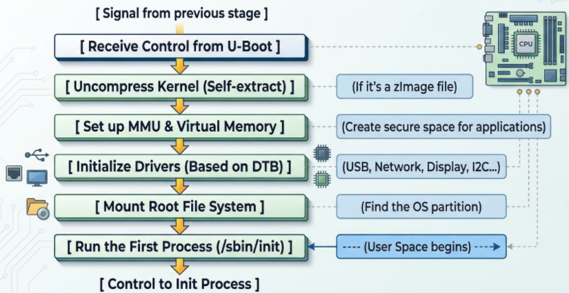
Linux Kernel schematic diagram
- The Linux kernel goes through several crucial steps to complete the system boot process:
First, the kernel initializes the MMU (Memory Management Unit) to convert from physical addresses to virtual addresses, isolating and protecting memory between applications, ensuring system stability even if a process fails. - Next, the kernel reads the Device Tree to load drivers and configure peripherals such as the display, network (TCP/IP for Ethernet/Wi-Fi), and industrial protocols (CAN, RS485).
- Then, the kernel attempts to mount the Root File System (rootfs) from storage devices such as SD cards or eMMCs; failure results in a “Kernel Panic” error. Upon successful mounting, the system executes the first process, /sbin/init (Systemd or BusyBox), marking the transition to User Space, where user applications begin running. Simultaneously, the kernel can also use the RemoteProc framework to load firmware and activate the Cortex-M4 core to run in parallel, handling real-time tasks while Linux processes higher-level tasks.
Linux Init process
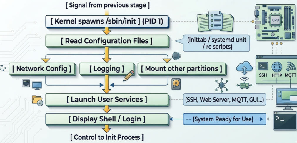
Linux Init process schematic diagram
When the kernel successfully mounts the RootFS partition (root file system), it finds and runs the first executable file. By default, this file is located at /sbin/init. The Init Process is the “parent” of all other processes in the Linux system. Its process identifier (PID) is always 1.
At this layer of the bootchain on the STM32MP1, running in user space, it executes network configuration scripts and starts applications (web server, Qt interface, or simply login commands).
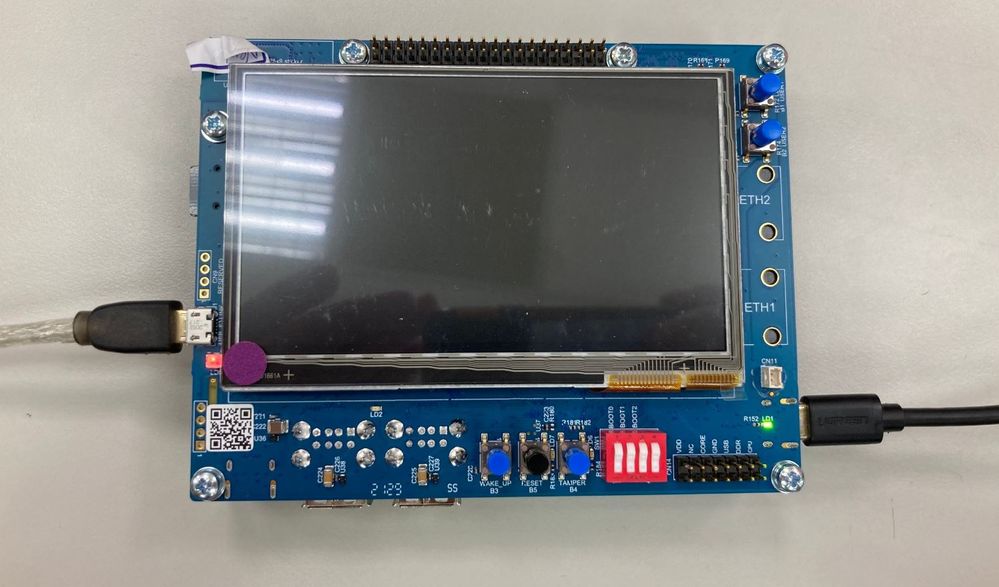
STM32MP135 DDR Configuration Using STM32DDRFW-UTIL
1. Introduction to STM32DDRFW-UTIL
2. Overview and Download of STM32DDRFW-UTIL
3. DDR Configuration Using STM32CubeMX
4. Configuring DDR Test Firmware
5. Flashing DDR Test Firmware Using STM32CubeProgrammer
6. Running DDR Memory Tests on STM32MP135
7. Conclusion
1. Introduction to STM32DDRFW-UTIL
STM32DDRFW-UTIL is a specialized firmware utility provided by STMicroelectronics designed for the initial bring-up and validation of DDR memory on STM32MP1 series microprocessors (including STM32MP135 and STM32MP157).
This utility acts as a bridge between the hardware and the STM32CubeProgrammer interface, allowing developers to:
- DDR Initialization: Configure the DDR controller and PHY timing parameters before the bootloader (FSBL/SSBL) is even loaded.
- Configuration Validation: Verify that the DDR settings generated in STM32CubeMX match the physical RAM chip specifications.
- Comprehensive Testing: Execute built-in diagnostic routines to ensure stability: Basic Tests, quick connectivity and data bus integrity checks. Intensive Tests, deep memory cell verification to catch intermittent bit flips. Stress Tests, high-load cycles to validate Signal Integrity (SI) and thermal stability.
- Hardware Debugging: Identify PCB routing issues, impedance mismatches, or power supply V_REF / V_TT fluctuations during the board bring-up phase.
2. Overview and download of STM32DDRFW-UTIL Tool
Link download: https://www.st.com/en/development-tools/stm32ddrfw-util.html
STM32DDRFW-UTIL is a toolkit provided by STMicroelectronics to support testing and evaluating the performance of DDR memory on STM32MP1 series microprocessors. This tool includes firmware tests, BSP libraries, HAL drivers, and sample projects for the STM32CubeIDE development environment. After downloading, users can build the firmware to create a .stm32 file, then flash it directly onto the board to perform RAM tests.
STM32DDRFW-UTIL offers various test types such as Basic test, Intensive test, and Stress test, allowing for testing of issues related to DDR configuration, timing, data bus, and memory stability. This enables engineers to detect hardware or configuration errors early during the bring-up process before the system boots up the bootloader or Linux operating system.
This toolkit can be downloaded directly from the STMicroelectronics development page. After downloading, users should extract the files and review the folder structure to understand the components, such as the firmware tests, sample projects, and DDR configuration files. This makes customizing the board easier and more accurate.
3. DDR Configuration Using STM32CubeMX
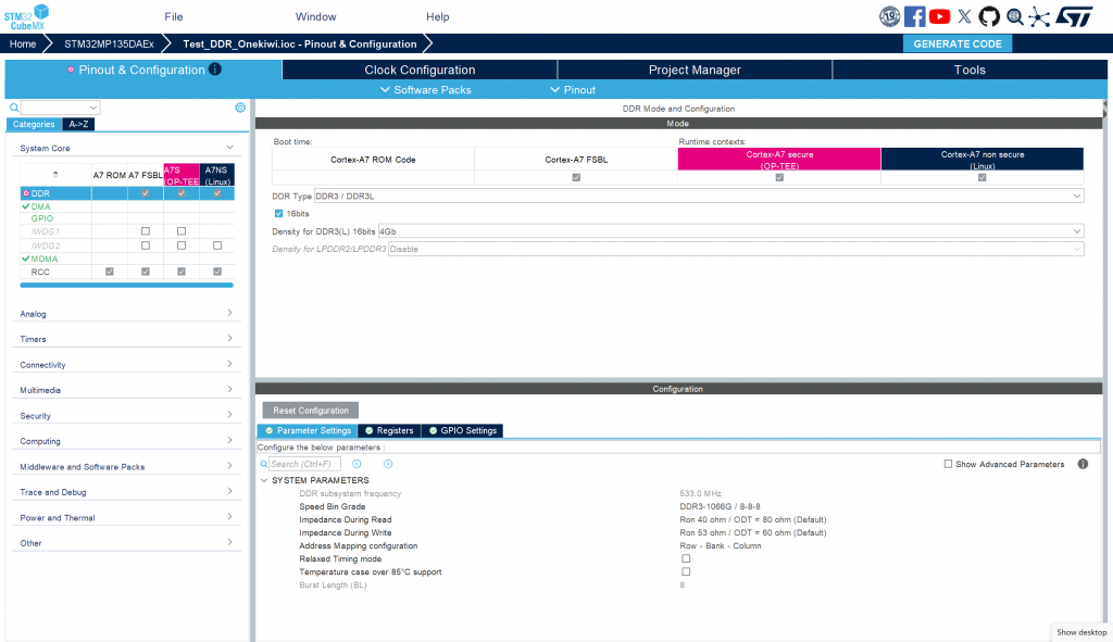
To configure DDR for the system, first open STM32CubeMX and select ACCESS TO MCU SELECTOR to search for the STM32MP135 processor. After selecting the correct MPU, create a new project. In the configuration interface, go to the System Core tab → DDR to set the memory parameters. Here, you need to select the correct type of RAM being used, for example, DDR3L Zentel A3T4GF40BBF. Next, switch to the Clock Configuration tab to configure the clock speed for the DDR controller. Set the value PLL2R = 533 MHz, which is the operating frequency of DDR. After completing the configuration steps, switch to the Project Manager tab and select GENERATE CODE to generate the source code. When the generation process is complete, access the folder …/<project_name>/DeviceTree/<project_name>/tf-a/ and find the stm32mp13-mx.dtsi file. This is a crucial file containing the complete configuration of DDR registers, used in the initialization and control of DDR memory on the system.
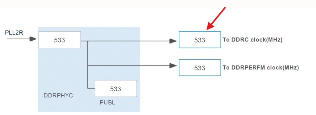
setting frequency in clock configuration
4. Configuring DDR Test Firmware
To configure the server firmware for DDR testing, first open STM32CubeIDE and import the project template STM32MP135C-DK. This is the project template provided for running the DDR Test Tool on the STM32MP135 processor line. After importing the project, it is necessary to check and adjust the PMIC configuration to match the board’s hardware. On the ST reference board, the system uses STPMIC with an I2C address of 0x33. However, for board customizations, the PMIC may be different, for example, using MP5470 with an I2C address of 0x11. Therefore, it is necessary to edit the corresponding parameters in the project’s configuration file, specifically stm32mp13xx_disco_bus.h and stm32mp13xx_util_conf.h, to ensure the firmware can correctly communicate with the PMIC and provide the correct level of power for DDR during testing.
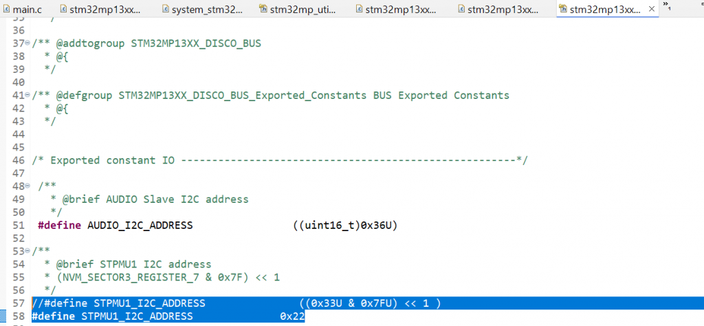
Refer to line 57 in stm32mp13xx_disco_bus.h
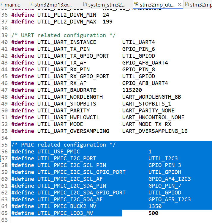
Change param in stm32mp_utils_conf.h
The following functions in main.c need to be modified: The SystemPower_Config() function is responsible for initializing the I2C interface to communicate with the PMIC and provide power to the RAM. While the STM32MP135C-DK performs strict checks, such as verifying the PMIC version, these steps are unnecessary for the Onekiwi board since it does not use an official ST PMIC. Therefore, these validation steps should be bypassed.
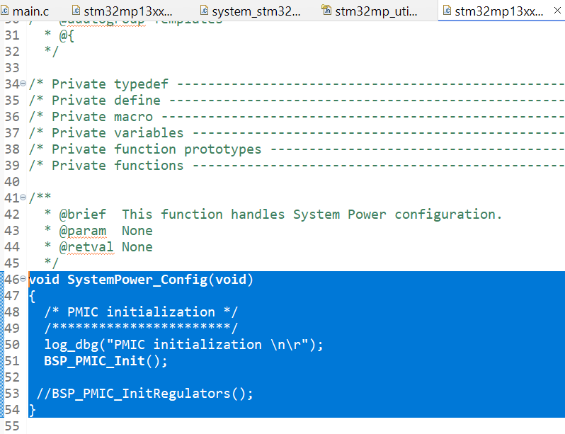
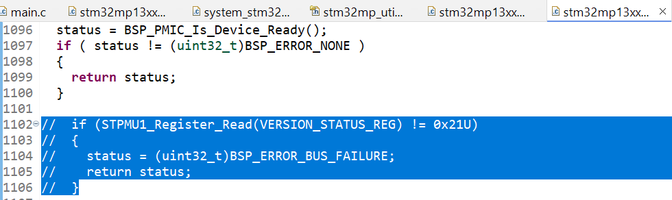
Comment out code in BSP_PMIC_Init()
The RAM configuration is handled in stm32mp13xx-ddr3-4Gb-template.h. Copy the contents of the stm32mp13-mx.dtsi file (generated from the previous RAM configuration step) and paste them into this header file. Once the configuration is accurately adjusted for the board, build the project and proceed to flash it onto the board.
5. Flashing DDR Test Firmware Using STM32CubeProgrammer
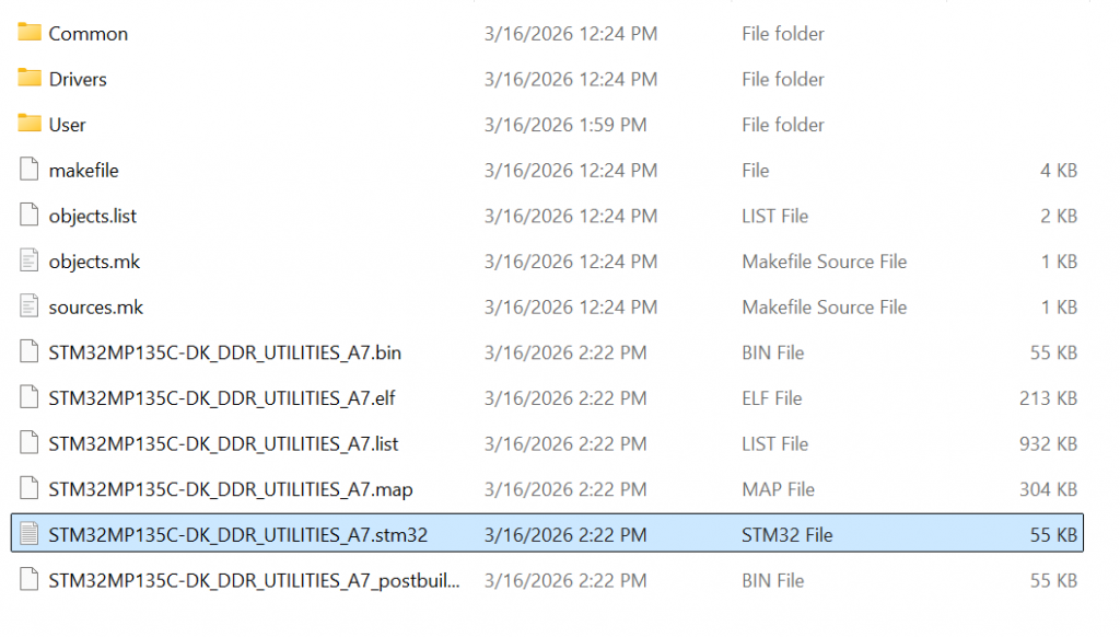
After the project build is complete in STM32CubeIDE, the system will create a firmware file in .stm32 format. This file is used to load the DDR Test Tool program onto the STM32MP135 microcontroller for RAM testing. Before flashing the firmware, connect the board to the computer via the USB Type-C port. Simultaneously, open a terminal, such as MobaXterm, to monitor logs from the board’s UART port during the tool’s execution. Next, use STM32CubeProgrammer to load the firmware. Open the CMD window and run the command: STM32_Programmer_CLI.exe -c port=USB1 -w “path_to_file.stm32” 0x01 -s 0x01
Ex: STM32_Programmer_CLI.exe -c port=USB1 -w “C:\Users\Admin\workspace\STM32DDRFW-UTIL\DDR_Tool\STM32MP135C-DK\STM32MP135C-DK_DDR_UTILITIES_A7\DK\STM32MP135C-DK_DDR_UTILITIES_A7.stm32” 0x01 -s 0x01
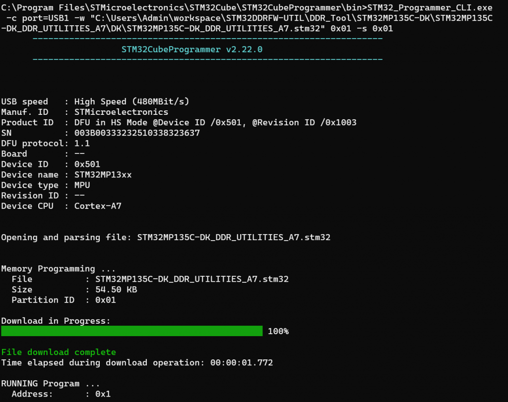
In this command, the “-w” parameter specifies the path to the newly built .stm32 file. After the command is successfully executed, the DDR test firmware will be loaded into the MPU, and the system will start running the DDR Utility Tool, ready to perform RAM testing commands.
6. Running DDR Memory Tests on STM32MP135
After the firmware is loaded and starts running on the STM32MP135, the MobaXterm terminal window will display a command prompt as shown in the image:
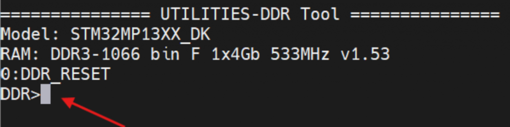
This prompt indicates that the DDR Utility Tool has successfully started and is ready to receive commands from the user. Here, you can enter commands to test and evaluate the performance of your DDR memory. For example, enter the command:
help

info

freq

...
To display a list of supported commands in the tool. Through these commands, users can view DDR configuration information, change parameters, and run RAM tests to confirm stable memory operation on the system. You can test using the following commands:
- Command info:
| Command-line | Expected result | Verdict |
|---|---|---|
| info | step = 0 : DDR_RESET | PASS |
| name = DDR3-1066/888 bin G 1x4Gb 533MHz v1.45 | ||
| size = 0x20000000 | ||
| speed = 533000 kHz | ||
| cal = 0 |
- Command freq:
| Command-line | Expected result | Verdict |
|---|---|---|
| freq | DDRPHY = 528000 kHz | PASS |
- Command param:
| Command-line | Expected result | Verdict |
|---|---|---|
| param | ==ctl.static== | PASS |
| mstr = 0x00040401 | ||
| mrctrl0 = 0x00000010 | ||
| mrctrl1 = 0x00000000 | ||
| derateen = 0x00000000 | ||
| derateint = 0x00800000 | ||
| pwrctl = 0x00000000 | ||
| pwrtmg = 0x00400010 | ||
| hwlpctl = 0x00000000 | ||
| rfshctl0 = 0x00210000 |
- Change parameter DDR:
| Command-line | Expected result | Verdict |
|---|---|---|
| param mstr | mstr = 0x00040401 | PASS |
| param mstr 0x00040402 | mstr = 0x00040402 | PASS |
| param mstr | mstr = 0x00040402 | PASS |
| param mstr 0x00040401 | mstr = 0x00040401 | PASS |
- State transition DDR:
| Command-line | Expected result | Verdict |
|---|---|---|
| next | 1 : DDR_CTRL_INIT_DONE | PASS |
| step 3 | step to 3 : DDR_READY | PASS |
| 1 : DDR_CTRL_INIT_DONE | ||
| 2 : DDR_PHY_INIT_DONE | ||
| 3 : DDR_READY |
- Command test RAM
| Command-line | Expected result | Verdict |
|---|---|---|
| test help | displays test commands | PASS |
| 0 : Test All | ||
| 1 : Test Simple DataBus |
- Test Data Bus
| Command-line | Expected result | Verdict |
|---|---|---|
| test 1 0xc0000000 | Result: Pass [Test Simple DataBus] | PASS |
- Test RAM
| Command-line | Expected result |
|---|---|
| test 0 | result 1: Test Simple DataBus = Passed |
| result 2: Test DataBusWalking0 = Passed | |
| result 3: Test DataBusWalking1 = Passed | |
| result 4: Test AddressBus = Passed | |
| result 5: Test MemDevice = Passed | |
| result 6: Test SimultaneousSwitchingOutput = Passed | |
| result 7: Test Noise = Passed | |
| result 8: Test NoiseBurst = Passed | |
| result 9: Test Random = Passed | |
| result 10: Test FrequencySelectivePattern = Passed | |
| result 11: Test BlockSequential = Passed | |
| result 12: Test Checkerboard = Passed | |
| result 13: Test BitSpread = Passed | |
| result 14: Test BitFlip = Passed | |
| result 15: Test WalkingZeroes = Passed | |
| result 16: Test WalkingOnes = Passed | |
| Result: Pass [Test All] |
7. Conclusion
The STM32DDRFW-UTIL toolkit provides an efficient and practical method for validating DDR memory during the early hardware bring-up stage of STM32MP135 and other STM32MP1 microprocessors from STMicroelectronics. By allowing developers to initialize DDR, verify configuration parameters generated by STM32CubeMX, and execute multiple memory diagnostic tests, the tool helps ensure that the DDR subsystem operates reliably before the system boots the bootloader or Linux operating system.
Through built-in commands and comprehensive testing routines—ranging from simple data bus verification to full stress testing—engineers can quickly identify potential issues such as incorrect DDR timing parameters, signal integrity problems, PCB routing errors, or unstable power supply conditions. This greatly simplifies the debugging process and reduces development time during the hardware validation phase.
In summary, integrating STM32DDRFW-UTIL into the development workflow enables engineers to confidently validate DDR hardware and configuration, ensuring a stable foundation for the entire embedded software stack.
Mastering Flash Memory: Architecture and Protocols
1. Flash Memory Overview
2. Flash Memory Protocol: SPI, QSPI, OSPI
2.1. Protocols in NOR Flash Memory
2.2. Protocols in NAND Flash Memory
2.3. NAND vs. NOR Interface Comparison
3. Conclusion
1. Flash Memory Overview
Flash memory is a type of non-volatile memory. This means that data is retained even when the device is powered off. Unlike many traditional memory types, Flash memory allows data to be erased and rewritten using electrical signals instead of requiring hardware replacement. Therefore, it has become a popular storage solution in modern electronic devices.
Today, Flash memory is widely used in many devices such as:
- USB flash drive
- SD/microSD memory card
- Smartphones
- Digital cameras
- Tablets and IoT devices
- SSD (Solid State Drive)
A major advantage of Flash Memory is that it has no moving mechanical parts, making it more durable, energy-efficient, and more resistant to vibration than traditional hard drives (HDDs). Flash Memory is currently divided into two main architectures: NOR Flash and NAND Flash; these two types differ in circuit structure, access speed, capacity, and intended use.
NOR FLASH MEMORY
In the image, you can see that each transistor (memory cell) has its drain terminal directly connected to the bit line (in the image, the vertical line connected to V_D) and its source terminal connected to ground (Gnd). This is characteristic of NOR architecture, allowing random access to each memory cell independently, creating a parallel structure.
Operating mechanism:
- When reading data from cell A, the system activates the central horizontal line (V_CG) and the central vertical line (V_D).
- If cell A contains electrons (currently storing 0), it will block current flow. If there are no electrons (currently storing 1), current will flow from $V_D$ to ground (Gnd).
- The sensor will measure this current to determine whether the cell is 0 or 1.
Due to its parallel design, data travels directly from the memory cell to the bit line. It has high reliability and is suitable for storing system source code (such as computer BIOS or phone firmware) because it is less prone to bit errors than NAND.
NAND FLASH MEMORY
Due to the serial design where transistors are connected to form a chain, data must “queue” through other cells to reach the bit path, making random access slower than NOR. However, thanks to this structure, NAND has enormous capacity and is inexpensive, making it extremely suitable for SSDs, USB drives, or memory cards – where we need to store huge amounts of data such as images, videos, and files.
Operating Mechanism:
- When reading data at cell B, the system activates the central horizontal line V_CG or WL1) with a specific reading voltage.
- Key Difference: Unselected cells in the same column (such as cells A and C) are forced to “open” (apply a high voltage V_pass) so that current can flow through them, regardless of what they contain.
- If cell B contains an electron (currently holding a 0), it will block the current of the entire chain. If cell B is empty (currently holding a 1), the current will flow freely from V_D, through A, through B, through C, and then to ground.
- The sensor will measure the current at the end of the chain to determine whether cell B’s value is 0 or 1.
Comparison between NAND Flash Memory vs NOR Flash Memory
| Feature | NAND Flash | NOR Flash |
|---|---|---|
| Memory Cell Connection | Cells connected in series (NAND structure) | Cells connected in parallel (NOR structure) |
| Access Method | Page-based read/write, block erase | Random access read, byte-level access |
| Read Speed | Moderate | Very fast |
| Write Speed | Fast | Slower than NAND |
| Erase Speed | Fast (block erase) | Slower |
| Storage Capacity | Very high (GB to TB range) | Lower capacity (usually MB to small GB) |
| Cost per Bit | Lower | Higher |
| Code Execution | Not suitable for direct code execution | Supports Execute In Place (XIP) |
| Reliability / Endurance | Lower endurance than NOR | Higher endurance |
| Typical Applications | SSD, USB drives, SD cards, smartphones | Firmware storage, BIOS, embedded systems |
2. Flash Memory Protocol: SPI, QSPI và OSPI
2.1. Protocols in NOR Flash Memory
SPI in NOR Flash Memory
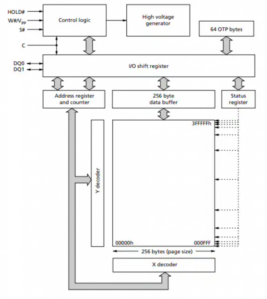
SPI NOR Flash is a popular type of Flash memory in embedded systems due to its simple interface design and high reliability. One of the key advantages of the SPI protocol is its multi-slave capability on the same bus. In this architecture, multiple Flash chips can share data lines and clock speeds, including MOSI, MISO, and SCLK. The microcontroller (Master) only needs to use a separate Chip Select (CS/SS) line for each device, thereby saving the number of GPIO pins on the microcontroller and simplifying the hardware design.
In terms of data transfer performance, SPI operates using a single-bit transfer mechanism, transmitting 1 bit of data per clock cycle. While this speed is sufficient for many basic embedded applications, in systems requiring higher bandwidth, the SPI protocol can be extended to Dual SPI (2 data lines) or Quad SPI (4 data lines) by utilizing additional functional pins of the Flash chip.
The standard SPI protocol is the most basic communication platform between a microcontroller and NOR Flash memory. It uses a synchronous serial data transmission and reception mechanism with a 4-wire main signal structure:
- SCLK (Serial Clock – Red): The synchronization clock generated by the Master. All data bit read/write operations are based on the timing of this clock.
- MOSI (Master Out Slave In – Green): The command and data transmission line from the Master to the Flash chip (e.g., sending read commands, erase commands, or memory addresses).
- MISO (Master In Slave Out – Blue): The data transmission line from the Flash chip back to the Master (e.g., the content of the data being read).
- SS/CS (Slave Select / Chip Select – Yellow): Chip selection signals (SS1, SS2, SS3 separate for each Slave). When communicating with a specific NOR Flash chip, the Master pulls the corresponding SS pin low (Logic 0). The remaining chips will be in a “sleep” state and ignore all signals on the common bus.
QSPI in NOR Flash Memory
Quad-SPI (QSPI) extends the SPI protocol by utilizing four bilateral data lines labeled IO0, IO1, IO2, and IO3. This allows QSPI to transmit 4 bits of data per clock cycle, increasing bandwidth by four times compared to standard SPI, which transmits only 1 bit per cycle. In normal SPI mode, some pins on the Flash chip have special functions such as Q2/nWP (Write Protect) and Q3/nHOLD (Hold). However, in Quad-SPI mode, these pins are reused as data lines, becoming IO2 and IO3.
In addition to data lines, QSPI still uses familiar control signals:
- CLK: data transmission synchronization clock
- nCS (Chip Select): signal to select the chip to operate at a low level
OSPI in NOR Flash Memory
The diagram shows how the Octal SPI Manager coordinates extremely complex signals to achieve maximum speed:
- 8 data lines (Data [7:0]): Divided into two groups (Data[3:0] and Data[4:7]). This allows simultaneous transmission of 8 bits (1 byte) in each clock cycle, doubling the bandwidth compared to QSPI.
- DQS (Data Strobe) pin: This is a “vital” component in the diagram. At extremely high speeds (above 100MHz), the clock signal is prone to phase shift. The DQS pin acts as a feedback signal from the Flash chip to the MCU to ensure that data is accurately sampled at the most stable point.
- Multi-port system (Port 1 & Port 2): The structure shown in the figure allows the MCU to communicate in parallel with two OSPI devices simultaneously, or flexibly manage between an OSPI NOR Flash chip and an OSPI RAM chip.
In terms of operation, OSPI completely changes the way data is transmitted through advanced modes such as SDR (1 byte/cycle transmission) and especially DDR/DTR (Double Data Rate) – allowing data transmission on both the rising and falling edges of the clock, pushing speeds up to 2 bytes/cycle. Despite its power, the OCTOSPIM controller maintains flexibility with backward compatibility, easily reconfigurable data pins to function as a conventional SPI or QSPI chip.
2.2. Protocols in NAND Flash Memory
SPI in NAND Flash Memory
There are a few key technical details that differentiate NAND and NOR, although both use the same SPI/QSPI interface:
- ECC (Error Correction Code) Block: This is the most obvious distinguishing feature. Because NAND Flash frequently experiences bit flips during use, it requires an integrated ECC error control unit. NOR Flash is much more stable and usually doesn’t need this block.
- Cache Memory: NAND Flash doesn’t allow direct byte-by-byte reading from the main memory array. Data must be loaded from the NAND array into a cache/page buffer before being pushed out via the SPI interface. Your diagram clearly illustrates this flow.
- Quad-SPI Interface: The signal pins at the top ($SIO0$ to $SIO3$) indicate that the chip supports Quad mode, which increases the data transfer speed for NAND (which has slower read speeds than NOR).
- Internal MCU: Some modern SPI NAND chips incorporate a small controller (MCU) inside to manage complex tasks such as bad block management and automatic ECC algorithms.
QSPI in NAND Flash Memory
The core difference in the operation of QSPI NAND compared to NOR is the two-stage data reading process.
- Stage 1: Page Read (From NAND Array to Cache): The MCU sends a page read command (Page Read) along with the address via the SPI protocol. Then, the NAND chip automatically reads data from the main storage array (NAND Array) and loads it into the internal Cache Register. This process takes a waiting time (busy time).
- Stage 2: Read From Cache (From Cache to MCU via QSPI): After the data is in the Cache, the MCU sends a read command from the cache. At this point, data is simultaneously pushed out on all four IO lines (IO0, IO1, IO2, IO3). With 4 bits transmitted per clock cycle, the speed is four times faster than traditional SPI.
OSPI in NAND Flash Memory
While traditional NAND Flash uses a complex parallel interface with many pins, modern embedded systems favor Serial NAND Flash (often called SPI NAND) due to its low pin count and simplified PCB design.
SPI & QSPI in NAND Flash
- SPI Mode: The basic communication mode using two data lines (SI and SO). It is reliable but limited in speed, suitable for low-bandwidth data logging.
- QSPI Mode (Quad-SPI): This is the most popular performance tier for SPI NAND. It repurposes the WP# and Hold# pins as additional data lines (IO2 and IO3). By transmitting 4 bits per clock cycle, QSPI significantly reduces the time needed to read large data blocks from the NAND cache to the MCU.
Why not OSPI in NAND?
Unlike NOR Flash, OSPI (Octal SPI) is extremely rare in NAND Flash. This is because the internal “Page Read” time of NAND is a physical bottleneck. Increasing the interface to 8 bits (OSPI) provides diminishing returns since the system still has to wait for the NAND array to move data into the cache.
2.3. NAND vs. NOR Interface Comparison
| Feature | NOR Flash | NAND Flash |
|---|---|---|
| Common Interface | SPI, QSPI, OSPI | SPI NAND, QSPI NAND |
| Main Purpose | Firmware storage | Mass data storage |
| Execute In Place (XIP) | Supported (especially with QSPI/OSPI) | Not supported |
| Data Access Type | Random access | Page-based access |
| Read Flow | Direct read from memory array | Read page to cache → read from cache |
| SPI Support | Very common | Common in SPI NAND |
| QSPI Support | Widely used for high-speed read | Used to speed up cache read |
| OSPI Support | Increasingly used in high-performance systems | Rarely used |
| Data Bus Width | 1-bit (SPI), 4-bit (QSPI), 8-bit (OSPI) | Usually 1-bit or 4-bit |
| Typical Clock Speed | Up to 133 MHz or higher | Usually lower than NOR |
| Implementation Complexity | Simple driver | More complex (ECC, bad block management) |
| Typical Applications | Bootloader, firmware, MCU code storage | SSD, eMMC, USB storage |
The choice depends on system priorities: Choose NOR Flash if you need fast random read speeds and absolute firmware security; choose NAND Flash if the top priority is large capacity and budget optimization. In practice, engineers often combine both: using a small NOR chip for booting and a large NAND chip to store all user data, creating a system that is both responsive and powerful.
3. Conclusion
Furthermore, the evolution of communication interfaces from standard SPI to high-performance QSPI and OSPI has significantly boosted data throughput, enabling modern embedded systems to handle complex tasks with smaller footprints. Understanding these architectural differences and protocol nuances is essential for any developer looking to balance performance, reliability, and cost in today’s evolving electronic landscape.