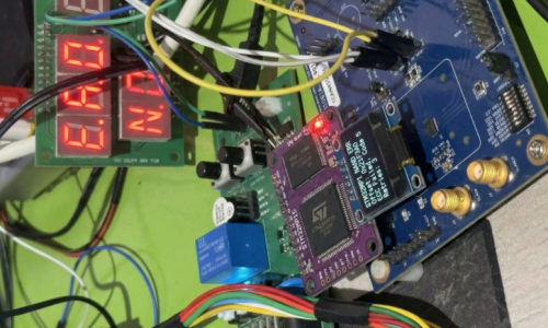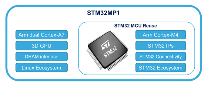
Bring-up Board STM32MP1
1. Bring-up steps
2. DDR Tuning & Stress Test
The Flashing Chain
Check Verify Issue
Bring-up Board STM32MP1
1. Bring-up steps
Step 1: Check the hardware baseline.
Before powering on, ensure that the basic physical parameters do not cause a short circuit.
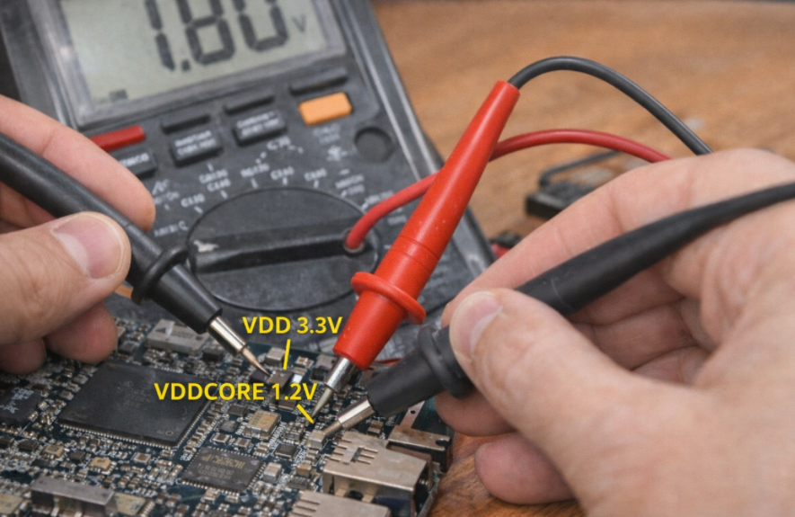
- Check the power supply: Use a multimeter (VOM) to measure the impedance of the main power lines (V_DDCORE, V_DD\_DDR, V_DD).
- Power on: Observe the board’s current consumption. If the current spikes (High current), disconnect the power immediately.
- Check the PMIC: Measure the output voltage at the capacitors surrounding the PMIC (STPMIC1). Ensure the voltage is 1.2V for the Core and 1.35V or 1.5V for the DDR.
Step 2: Set up Boot Pins (Boot Configuration)
1. Principles of Interfering with BootROM Logic
Each microprocessor, upon leaving the factory, has a fixed, unchangeable piece of code called BootROM. When power is applied, BootROM scans the voltage state (Logic High/Low) on dedicated configuration pins such as BOOT0, BOOT1, and BOOT2.
- Mechanism: Flipping the switches (DIP switches) or changing the pull-up/pull-down resistors sends an “encoding signal” to the microprocessor.
- Purpose: To instruct the chip to skip searching for software in the internal storage memory (which is usually empty) and go straight to waiting for commands from external communication ports.
2. USB OTG Priority Mode (DFU Mode)
For the STM32MP1 series, the binary configuration is usually set to 000 (or according to the manufacturer’s specific reference diagram) to prioritize USB OTG (Device) mode.
- DFU (Device Firmware Upgrade): In this mode, the processor acts as a slave device. As soon as it connects to the Host PC via a USB Type-C cable, the BootROM will initialize a minimal USB stack so that the computer can recognize the device as a “USB DFU Device”. This is the state that allows the STM32CubeProgrammer tool to “see” the chip and be ready to transfer data.
3. Physical Bring-up Chain Diagram
To ensure stable and reliable data transmission, the bring-up chain diagram must adhere to the following structure:
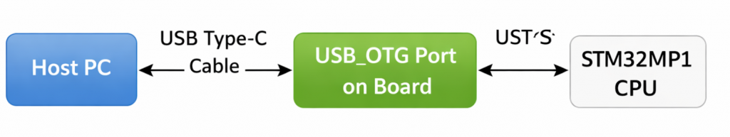
In this connection chain, the USB_OTG port acts as the sole gateway. Correctly configuring the BOOT pins “opens” this gateway, allowing data from the computer to go directly to the lowest hardware layer of the CPU without passing through any running operating system.
Step 3: Check the connection with the Host PC (DFU Mode)
When you connect the device to the computer and select the USB interface in the STM32CubeProgrammer tool, a digital “handshake” process takes place. If the BOOT pin configuration in the previous step was correct, the chip’s BootROM will send identification parameters (Vendor ID and Product ID) to the computer. When you press Connect, the software will query the chip’s unique Serial Number and display the “Connected” status.
Technical Significance of a Successful Connection
A stable connection is practical proof that the Minimum Operating Conditions have been met:
- CPU “Live”: The main logic block of the microprocessor is active and executing code from the BootROM.
- Power System (PMIC/LDO): The core power lines (VDD, VDDCORE, VDD_USB) are providing stable voltage, without voltage drops or interference.
- Oscillator (Clocking): The quartz crystal (usually 24MHz) is oscillating accurately, allowing the frequency multiplier (PLL) inside the chip to generate the necessary clock pulse for the USB controller.
Analyzing the Cause of Connection Failure
If the computer reports “USB Device Not Recognized” or the device is not found, this is a warning signal of a physical error on the hardware layer:
- Clock Error: If the 24MHz quartz crystal is not working or is at the wrong frequency, the USB controller will be unable to synchronize data with the Host PC, resulting in the device being “invisible” to the software.
- Signal Integrity: The USB D+/D- differential signal pair needs to be checked. Even a small design flaw (such as unbalanced 90 Ohm impedance) or a mechanical contact error will interrupt the data flow.
- Boot Status: The CPU may still be stuck in Flash boot mode instead of entering Load Mode (DFU), requiring a check of the logic levels on the BOOT0/1/2 pins.
2. DDR Tuning & Stress Test
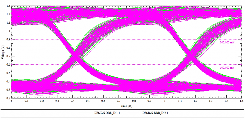
Eye Diagram for DDR
During the DDR bring-up process, simply checking if the RAM is fully recognized isn’t enough. We need to observe the Eye Diagram.
- If the ‘eye’ is wide and clean: The signal is extremely stable, the Timing and Voltage Swing parameters are optimized, and the system will run reliably 24/7 without crashing.
- If the ‘eye’ is narrow or noisy (Closed eye): This means the PCB traces are too long, there’s crosstalk, or the Drive Strength configuration is incorrect. This is the cause of random kernel panics that are very difficult to debug later.
The image above shows an Eye Diagram of a DDR signal, created by overlaying multiple signal cycles in the time domain. The horizontal axis represents time (ns), while the vertical axis represents voltage (V), allowing for simultaneous evaluation of the signal’s timing and amplitude characteristics. The “eye opening” represents the time and voltage range at which data can be safely sampled. A clear, wide eye indicates a signal with low noise, small jitter, and good timing margin, thus ensuring stable high-speed data transmission on the DDR bus. The pink and green signal lines represent multiple samples of different data bits, overlaid to reflect the actual signal variation. The reference voltage level lines (e.g., ~0.6V and ~0.9V) serve as logical thresholds, helping to determine the ability to distinguish between ‘0’ and ‘1’ levels. This diagram is a crucial tool in the bring-up and optimization process, especially when evaluating DDR signal quality. A properly calibrated Eye Diagram is essential to ensuring accurate and reliable DDR initialization and data transfer.
After the computer recognizes the chip, the next step in bring-up is to get the RAM working. If the RAM is faulty, you will never be able to boot Linux.
- Tool: Use the DDR Tool tab in STM32CubeMX.
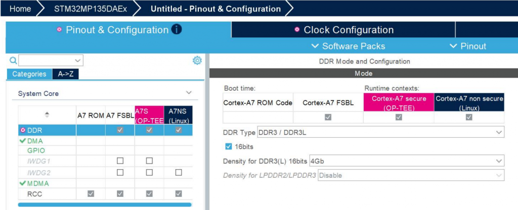
- Procedure:
- Load the RAM configuration file (DDR3/LPDDR3) into the tool.
- Click Test: The tool will load a small piece of code into the SRAM to test the read/write capabilities of the external RAM
- DDR Training: The system automatically calculates the latency (skew) of the signal lines on the PCB to provide the optimal set of parameters.
The Flashing Chain
Because the SRAM of the STM32MP1 is very small, we cannot directly load an image file of several hundred MB into Flash memory. The process must be done in a “bridging” fashion: loading the small programmer to power the larger programmer, and then loading the actual data.
Step 1: Prepare the FlashLayout file (.tsv)
The configuration file (usually a Flash Layout) acts as the orchestrator of the entire system loading process, establishing key operating parameters for the loading tool. First, this file configures the physical layer by defining the connection protocol (USB/UART) to establish data flow between the Host PC and the Target. The core of the file is the Partition Map, which details the ID identifiers, system partition names (such as ssbl, boot, rootfs), and addresses mapped from executable files (.stm32, .bin) on the computer to the target memory.
A standard partition structure is established in a hierarchical logical sequence to ensure a reliable boot sequence: starting with the FSBL (TF-A) responsible for low-level hardware initialization, followed by the SSBL (U-Boot) acting as the second-stage loader, then the Boot Partition (containing the Kernel and DTB), and finally the RootFS (User Space) storage space. By tightly managing these indices, the flashing process ensures data integrity and consistency in the partition structure on the storage device.

Step 2: Load the primer phase (DFU phase)
In the architecture of application-oriented microprocessors like the STM32MP1, when the system has no software in its internal memory (eMMC/SD), it enters a state of “empty” control resources. The Primer phase is a crucial intermediate step to establish the execution environment in RAM before data can be written to Flash.
1. Loading TF-A (FSBL) into Internal SRAM: Initializing the Physical Layer
When the “Download” command is triggered from the STM32CubeProgrammer, the first process is to push the TF-A (Trusted Firmware-A) file, the version supporting the USB protocol, into the Internal SRAM.
- Principle: Because at boot time, the external DDR RAM is not yet configured and cannot be used, the system is forced to utilize the SRAM integrated within the chip (limited capacity but available power and instantaneous access).
- Key Task: As soon as it’s loaded into SRAM, the TF-A performs the most important task: configuring the DDR RAM controller and setting the voltage and clock speed parameters for the external RAM module. This is the “opening step” to provide the system with sufficient temporary storage space for the subsequent steps.
2. Loading U-Boot (SSBL) into DDR RAM: Setting up the storage controller
After the TF-A confirms the DDR RAM is ready for operation, the computer pushes the U-Boot file (usually in .stm32 format) into this DDR RAM memory.
- Principle: Unlike the TF-A, which focuses only on low-level hardware initialization, the U-Boot is a second-stage loader (SSBL) with a rich driver system.
- Key task: When U-Boot is executed from DDR RAM, it activates more complex communication protocols such as SDMMC (for SD/eMMC cards) or QSPI. At this point, the processor officially becomes capable of “understanding” and “communicating” with Flash memory.
3. The Role of the DFU “Bridge”
At the end of the Primer Phase, the device has transformed from a rudimentary hardware block into a system with full resource control:
- SRAM acts as the bootstrap.
- DDR RAM acts as a large-capacity data buffer.
- U-Boot acts as the “manager,” executing write commands directly from the USB data stream to the blocks on the eMMC/SD Card.
When you click “Download” on STM32CubeProgrammer:
- Load TF-A into SRAM: The USB version of the TF-A file is pushed into SRAM. The chip starts running TF-A to initialize DDR RAM.
- Load U-Boot into DDR: After the RAM is loaded, the computer pushes the U-Boot file (usually u-boot-stm32mp1…stm32) into DDR. At this point, U-Boot takes control and activates the eMMC/SD Card drivers.
Step 3: Write the data to storage memory.
U-Boot will open a “channel” to receive data from the computer via USB and write it directly to the partitions on the eMMC/SD Card according to the scheme in the .tsv file.
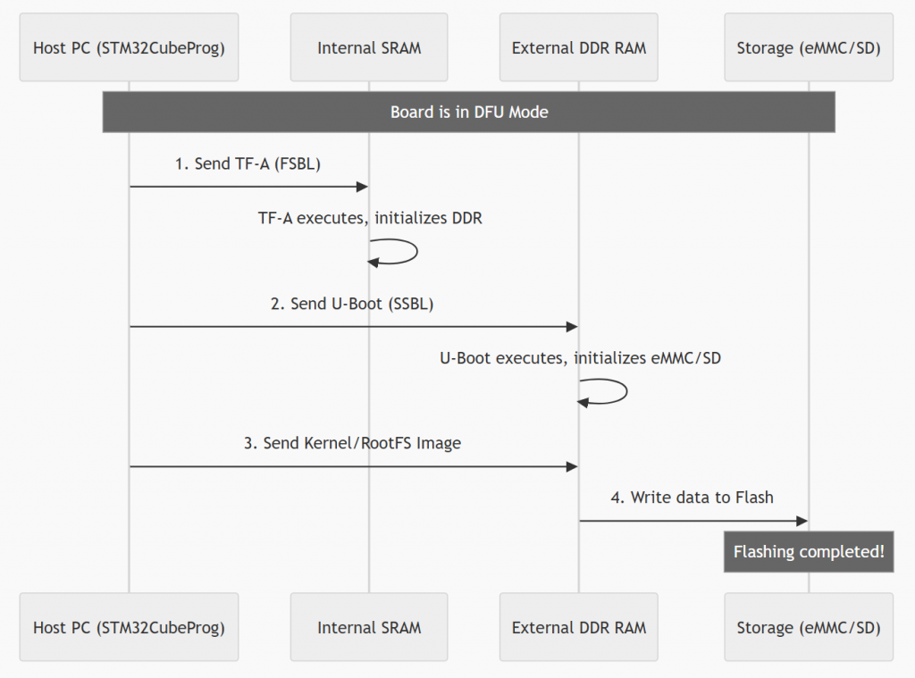
Flashing Process Diagram (Sequence Diagram)
The process shown in the image illustrates the flashing steps for an embedded system (typically the STM32MP1 series) via DFU (Device Firmware Upgrade) mode. This process is performed using a step-by-step “priming” mechanism to gradually initialize complex hardware components.
First, when the device is in DFU mode, the host PC sends the first-stage bootloader (TF-A/FSBL) to the internal SRAM. After the TF-A executes and activates the external DDR RAM, the PC continues to send the second-stage bootloader (U-Boot/SSBL) to it. At this point, U-Boot acts as a controller to initiate communication with storage devices such as eMMC or SD cards. Finally, larger operating system files (such as Kernel or RootFS) are loaded into DDR RAM and then officially written to Flash memory. The process ends when all data has been successfully loaded into permanent storage, allowing the device to boot up independently afterward.
Check verify issue
The golden rule: “The earlier the error appears, the closer the problem is to the hardware.” We will divide this into four main bottlenecks corresponding to the four boot stages.
- Issue 1: No Boot Log
- Issue 2: Freezes at FSBL (DDR/RAM Error)
- Issue 3: Hanging at SSBL (Storage/MMC Error)
- Issue 4: Kernel Panic (Linux Kernel & RootFS Error)
The systematization of the Bring-up process is not just a set of individual tests, but a logical process that strictly adheres to the Hardware Boot Chain. The core principle is hierarchical diagnostics: validating minimum operating conditions at the low level before expanding to more complex peripherals.
Each issue analyzed, from the silence of the No Boot Log to the crash of the Kernel Panic, marks a specific stop point (hang) in the boot process. To visualize the diagnostic priority order and how these issues are distributed across architectural layers, the diagnostic diagram below provides an overview of the boot event sequence.
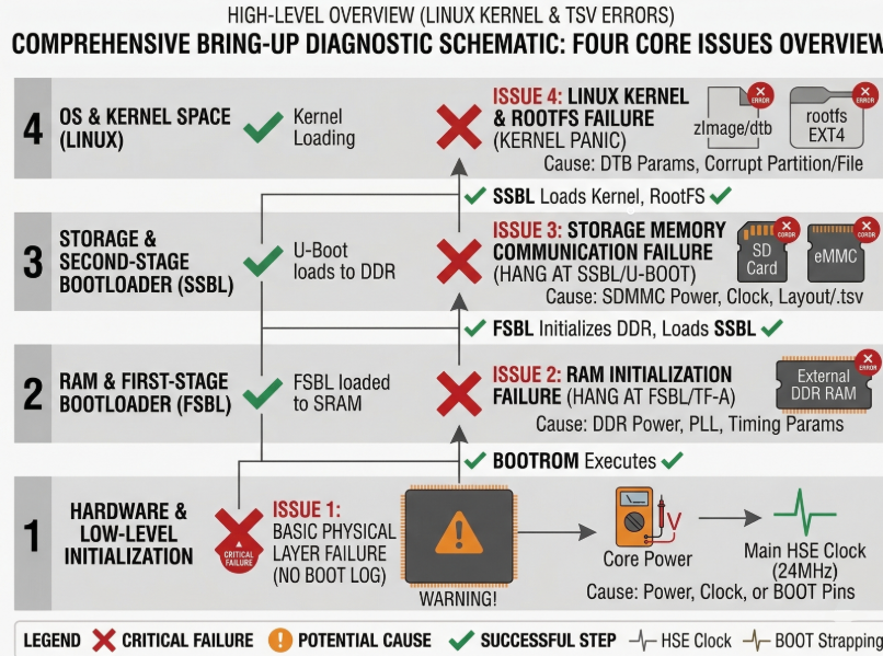
The diagram above clearly establishes a hierarchical diagnostic structure, progressing from the lowest Hardware & Low-level layer to the highest OS & Kernel Space layer. Red X marks indicate failed execution stages triggered by specific potential causes, while green checkmarks confirm successful execution steps.
This diagram serves as a quick diagnostic tool to pinpoint the problematic architecture layer. However, to transition from identifying errors (e.g., Treo at the Storage layer) to implementing specific technical solutions, a detailed action checklist is needed. The summary table below systematizes this visual diagram into a technical checklist, defining the components to be checked, the necessary tools, and specific implementation solutions for each error layer.
| Priority | Issue | Symptom Description | Component to Check | Checking Tool/Method | Specific Solution |
| 1 | Issue 1: Basic Physical Layer Failure (No Boot Log) | Board is completely silent. UART does not log. PC does not recognize USB DFU. |
1. Power Tree.
2. Clocking (24MHz HSE).
3. BOOT Configuration Pins (BOOT[2:0]). |
– Multimeter.
– Oscilloscope.
– Observe Switches/Resistors. |
– Measure VDDCORE, VDD_DDR, VDD.
– Measure crystal waveform.
– Set BOOT Switches to 000 (DFU). |
| 2 | Issue 2: RAM Initialization Failure (Hang at FSBL/TF-A) | Initial logs appear (BootROM/FSBL), then hangs completely. Last log is typically ‘DDR Initialization’. |
1. DDR PHY VDD (Power for RAM physical layer).
2. DDR Clock Tree (PLL_DDR).
3. DDR Parameters (Layout TSV / Device Tree |
– Multimeter (measure voltage drop).
– Refer to documentation (Datasheet, Schematic).
– TSV configuration file. |
– Check for stable VDD_DDR power.
– Check PLL_DDR in DTB.
– Compare DDR Timing Params with the RAM chip datasheet. |
| 3 | Issue 3: Storage Memory Communication Failure (Hang at SSBL/U-Boot) | U-Boot runs successfully, recognizes RAM, but hangs when attempting to access SD/eMMC. Last log is ‘Mounting’ or ‘Failed to read partition’. |
1. SDMMC VDD/VCC (Power for SD card/eMMC).
2. SDMMC Clock Tree.
3. Driver Configuration (U-Boot DTB / Flash Layout |
– Multimeter.
– Check TSV file for partition location.
– Check U-Boot Device Tree |
– Ensure SDMMC power is operational.
– Check
– Validate partition ID/address in the |
| 4 | Issue 4: Linux Kernel & RootFS Failure (Kernel Panic) | U-Boot successfully loads Kernel/DTB. Kernel begins to run, then crashes (Panic). Console displays ‘Kernel Panic’, ‘VFS: Unable to mount root fs’. |
1. Kernel Image Integrity (Data Corruption).
2. Kernel DTB Configuration (Incorrect DTB parameters).
3. RootFS Integrity (RootFS partition corruption). |
– Checksum (MD5/SHA).
– Look up
– Check EXT4 format of the RootFS. |
– Verify checksum of Kernel/RootFS files.
– Modify
– Attempt to recreate the RootFS partition ( |