1. Flash Memory Overview
2. Flash Memory Protocol: SPI, QSPI, OSPI
2.1. Protocols in NOR Flash Memory
2.2. Protocols in NAND Flash Memory
2.3. NAND vs. NOR Interface Comparison
3. Conclusion
1. Flash Memory Overview
Flash memory is a type of non-volatile memory. This means that data is retained even when the device is powered off. Unlike many traditional memory types, Flash memory allows data to be erased and rewritten using electrical signals instead of requiring hardware replacement. Therefore, it has become a popular storage solution in modern electronic devices.
Today, Flash memory is widely used in many devices such as:
- USB flash drive
- SD/microSD memory card
- Smartphones
- Digital cameras
- Tablets and IoT devices
- SSD (Solid State Drive)
A major advantage of Flash Memory is that it has no moving mechanical parts, making it more durable, energy-efficient, and more resistant to vibration than traditional hard drives (HDDs). Flash Memory is currently divided into two main architectures: NOR Flash and NAND Flash; these two types differ in circuit structure, access speed, capacity, and intended use.
NOR FLASH MEMORY
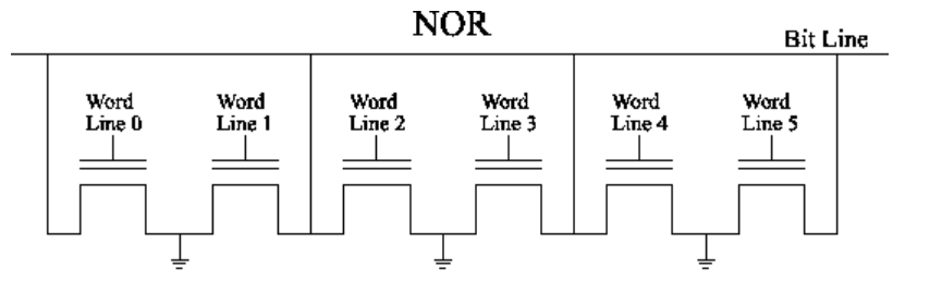
In the image, you can see that each transistor (memory cell) has its drain terminal directly connected to the bit line (in the image, the vertical line connected to V_D) and its source terminal connected to ground (Gnd). This is characteristic of NOR architecture, allowing random access to each memory cell independently, creating a parallel structure.
Operating mechanism:
- When reading data from cell A, the system activates the central horizontal line (V_CG) and the central vertical line (V_D).
- If cell A contains electrons (currently storing 0), it will block current flow. If there are no electrons (currently storing 1), current will flow from $V_D$ to ground (Gnd).
- The sensor will measure this current to determine whether the cell is 0 or 1.
Due to its parallel design, data travels directly from the memory cell to the bit line. It has high reliability and is suitable for storing system source code (such as computer BIOS or phone firmware) because it is less prone to bit errors than NAND.
NAND FLASH MEMORY
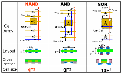
Due to the serial design where transistors are connected to form a chain, data must “queue” through other cells to reach the bit path, making random access slower than NOR. However, thanks to this structure, NAND has enormous capacity and is inexpensive, making it extremely suitable for SSDs, USB drives, or memory cards – where we need to store huge amounts of data such as images, videos, and files.
Operating Mechanism:
- When reading data at cell B, the system activates the central horizontal line V_CG or WL1) with a specific reading voltage.
- Key Difference: Unselected cells in the same column (such as cells A and C) are forced to “open” (apply a high voltage V_pass) so that current can flow through them, regardless of what they contain.
- If cell B contains an electron (currently holding a 0), it will block the current of the entire chain. If cell B is empty (currently holding a 1), the current will flow freely from V_D, through A, through B, through C, and then to ground.
- The sensor will measure the current at the end of the chain to determine whether cell B’s value is 0 or 1.
Comparison between NAND Flash Memory vs NOR Flash Memory
| Feature | NAND Flash | NOR Flash |
|---|---|---|
| Memory Cell Connection | Cells connected in series (NAND structure) | Cells connected in parallel (NOR structure) |
| Access Method | Page-based read/write, block erase | Random access read, byte-level access |
| Read Speed | Moderate | Very fast |
| Write Speed | Fast | Slower than NAND |
| Erase Speed | Fast (block erase) | Slower |
| Storage Capacity | Very high (GB to TB range) | Lower capacity (usually MB to small GB) |
| Cost per Bit | Lower | Higher |
| Code Execution | Not suitable for direct code execution | Supports Execute In Place (XIP) |
| Reliability / Endurance | Lower endurance than NOR | Higher endurance |
| Typical Applications | SSD, USB drives, SD cards, smartphones | Firmware storage, BIOS, embedded systems |
2. Flash Memory Protocol: SPI, QSPI và OSPI
2.1. Protocols in NOR Flash Memory
SPI in NOR Flash Memory
SPI NOR Flash is a popular type of Flash memory in embedded systems due to its simple interface design and high reliability. One of the key advantages of the SPI protocol is its multi-slave capability on the same bus. In this architecture, multiple Flash chips can share data lines and clock speeds, including MOSI, MISO, and SCLK. The microcontroller (Master) only needs to use a separate Chip Select (CS/SS) line for each device, thereby saving the number of GPIO pins on the microcontroller and simplifying the hardware design.
In terms of data transfer performance, SPI operates using a single-bit transfer mechanism, transmitting 1 bit of data per clock cycle. While this speed is sufficient for many basic embedded applications, in systems requiring higher bandwidth, the SPI protocol can be extended to Dual SPI (2 data lines) or Quad SPI (4 data lines) by utilizing additional functional pins of the Flash chip.
The standard SPI protocol is the most basic communication platform between a microcontroller and NOR Flash memory. It uses a synchronous serial data transmission and reception mechanism with a 4-wire main signal structure:
- SCLK (Serial Clock – Red): The synchronization clock generated by the Master. All data bit read/write operations are based on the timing of this clock.
- MOSI (Master Out Slave In – Green): The command and data transmission line from the Master to the Flash chip (e.g., sending read commands, erase commands, or memory addresses).
- MISO (Master In Slave Out – Blue): The data transmission line from the Flash chip back to the Master (e.g., the content of the data being read).
- SS/CS (Slave Select / Chip Select – Yellow): Chip selection signals (SS1, SS2, SS3 separate for each Slave). When communicating with a specific NOR Flash chip, the Master pulls the corresponding SS pin low (Logic 0). The remaining chips will be in a “sleep” state and ignore all signals on the common bus.
QSPI in NOR Flash Memory
Quad-SPI (QSPI) extends the SPI protocol by utilizing four bilateral data lines labeled IO0, IO1, IO2, and IO3. This allows QSPI to transmit 4 bits of data per clock cycle, increasing bandwidth by four times compared to standard SPI, which transmits only 1 bit per cycle. In normal SPI mode, some pins on the Flash chip have special functions such as Q2/nWP (Write Protect) and Q3/nHOLD (Hold). However, in Quad-SPI mode, these pins are reused as data lines, becoming IO2 and IO3.
In addition to data lines, QSPI still uses familiar control signals:
- CLK: data transmission synchronization clock
- nCS (Chip Select): signal to select the chip to operate at a low level
OSPI in NOR Flash Memory
The diagram shows how the Octal SPI Manager coordinates extremely complex signals to achieve maximum speed:
- 8 data lines (Data [7:0]): Divided into two groups (Data[3:0] and Data[4:7]). This allows simultaneous transmission of 8 bits (1 byte) in each clock cycle, doubling the bandwidth compared to QSPI.
- DQS (Data Strobe) pin: This is a “vital” component in the diagram. At extremely high speeds (above 100MHz), the clock signal is prone to phase shift. The DQS pin acts as a feedback signal from the Flash chip to the MCU to ensure that data is accurately sampled at the most stable point.
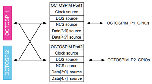
- Multi-port system (Port 1 & Port 2): The structure shown in the figure allows the MCU to communicate in parallel with two OSPI devices simultaneously, or flexibly manage between an OSPI NOR Flash chip and an OSPI RAM chip.
In terms of operation, OSPI completely changes the way data is transmitted through advanced modes such as SDR (1 byte/cycle transmission) and especially DDR/DTR (Double Data Rate) – allowing data transmission on both the rising and falling edges of the clock, pushing speeds up to 2 bytes/cycle. Despite its power, the OCTOSPIM controller maintains flexibility with backward compatibility, easily reconfigurable data pins to function as a conventional SPI or QSPI chip.
2.2. Protocols in NAND Flash Memory
SPI in NAND Flash Memory
There are a few key technical details that differentiate NAND and NOR, although both use the same SPI/QSPI interface:
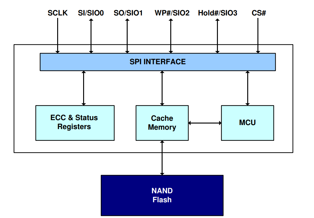
- ECC (Error Correction Code) Block: This is the most obvious distinguishing feature. Because NAND Flash frequently experiences bit flips during use, it requires an integrated ECC error control unit. NOR Flash is much more stable and usually doesn’t need this block.
- Cache Memory: NAND Flash doesn’t allow direct byte-by-byte reading from the main memory array. Data must be loaded from the NAND array into a cache/page buffer before being pushed out via the SPI interface. Your diagram clearly illustrates this flow.
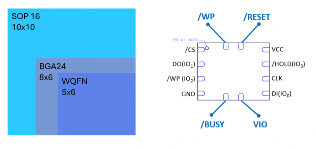
- Quad-SPI Interface: The signal pins at the top ($SIO0$ to $SIO3$) indicate that the chip supports Quad mode, which increases the data transfer speed for NAND (which has slower read speeds than NOR).
- Internal MCU: Some modern SPI NAND chips incorporate a small controller (MCU) inside to manage complex tasks such as bad block management and automatic ECC algorithms.
QSPI in NAND Flash Memory
The core difference in the operation of QSPI NAND compared to NOR is the two-stage data reading process.
- Stage 1: Page Read (From NAND Array to Cache): The MCU sends a page read command (Page Read) along with the address via the SPI protocol. Then, the NAND chip automatically reads data from the main storage array (NAND Array) and loads it into the internal Cache Register. This process takes a waiting time (busy time).
- Stage 2: Read From Cache (From Cache to MCU via QSPI): After the data is in the Cache, the MCU sends a read command from the cache. At this point, data is simultaneously pushed out on all four IO lines (IO0, IO1, IO2, IO3). With 4 bits transmitted per clock cycle, the speed is four times faster than traditional SPI.
OSPI in NAND Flash Memory
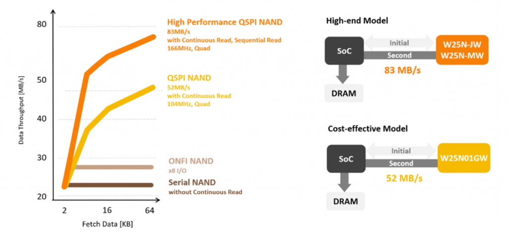
While traditional NAND Flash uses a complex parallel interface with many pins, modern embedded systems favor Serial NAND Flash (often called SPI NAND) due to its low pin count and simplified PCB design.
SPI & QSPI in NAND Flash
- SPI Mode: The basic communication mode using two data lines (SI and SO). It is reliable but limited in speed, suitable for low-bandwidth data logging.
- QSPI Mode (Quad-SPI): This is the most popular performance tier for SPI NAND. It repurposes the WP# and Hold# pins as additional data lines (IO2 and IO3). By transmitting 4 bits per clock cycle, QSPI significantly reduces the time needed to read large data blocks from the NAND cache to the MCU.
Why not OSPI in NAND?
Unlike NOR Flash, OSPI (Octal SPI) is extremely rare in NAND Flash. This is because the internal “Page Read” time of NAND is a physical bottleneck. Increasing the interface to 8 bits (OSPI) provides diminishing returns since the system still has to wait for the NAND array to move data into the cache.
2.3. NAND vs. NOR Interface Comparison
| Feature | NOR Flash | NAND Flash |
|---|---|---|
| Common Interface | SPI, QSPI, OSPI | SPI NAND, QSPI NAND |
| Main Purpose | Firmware storage | Mass data storage |
| Execute In Place (XIP) | Supported (especially with QSPI/OSPI) | Not supported |
| Data Access Type | Random access | Page-based access |
| Read Flow | Direct read from memory array | Read page to cache → read from cache |
| SPI Support | Very common | Common in SPI NAND |
| QSPI Support | Widely used for high-speed read | Used to speed up cache read |
| OSPI Support | Increasingly used in high-performance systems | Rarely used |
| Data Bus Width | 1-bit (SPI), 4-bit (QSPI), 8-bit (OSPI) | Usually 1-bit or 4-bit |
| Typical Clock Speed | Up to 133 MHz or higher | Usually lower than NOR |
| Implementation Complexity | Simple driver | More complex (ECC, bad block management) |
| Typical Applications | Bootloader, firmware, MCU code storage | SSD, eMMC, USB storage |
The choice depends on system priorities: Choose NOR Flash if you need fast random read speeds and absolute firmware security; choose NAND Flash if the top priority is large capacity and budget optimization. In practice, engineers often combine both: using a small NOR chip for booting and a large NAND chip to store all user data, creating a system that is both responsive and powerful.
3. Conclusion
Furthermore, the evolution of communication interfaces from standard SPI to high-performance QSPI and OSPI has significantly boosted data throughput, enabling modern embedded systems to handle complex tasks with smaller footprints. Understanding these architectural differences and protocol nuances is essential for any developer looking to balance performance, reliability, and cost in today’s evolving electronic landscape.