


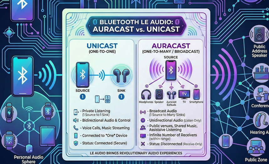
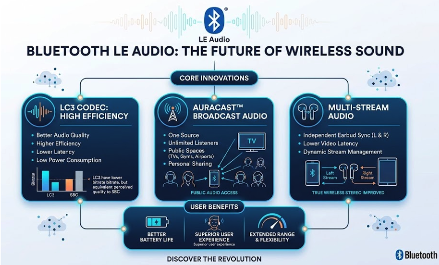

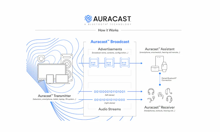
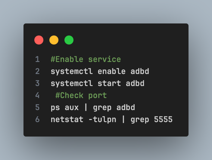
 An Auracast Source is a device that acts as an audio broadcast transmitter. It encodes the audio signal using LC3, then creates a BIG containing one or more BISs to transmit audio data at fixed intervals. Information about the broadcast stream is published via Extended Advertising and Periodic Advertising, allowing receiving devices to detect and synchronize. In some cases, the broadcast stream can be encrypted to restrict unauthorized access. Typical devices acting as an Auracast Source include public TVs, conference audio systems, airport transmitters, or an audio gateway in an embedded system. Importantly, the Source does not need to manage each individual receiving device, making the system highly scalable.


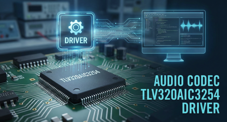
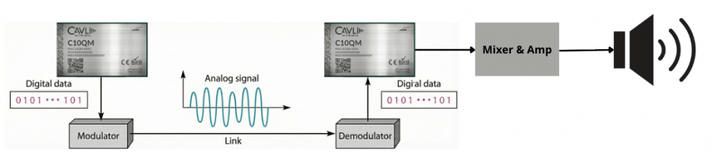
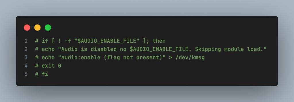
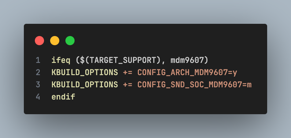
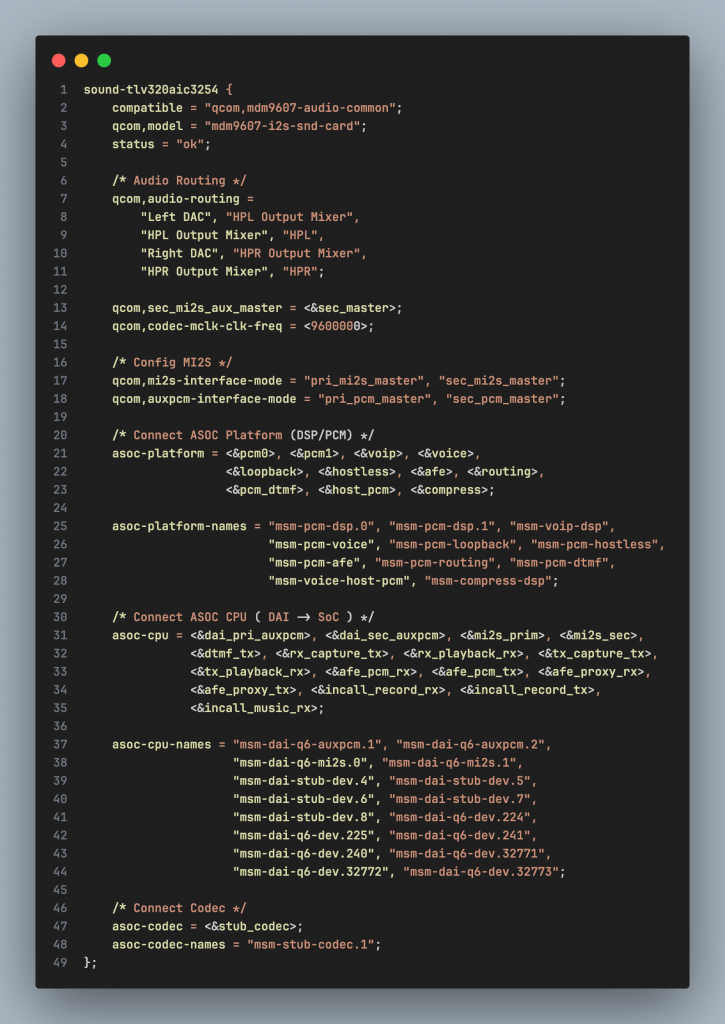
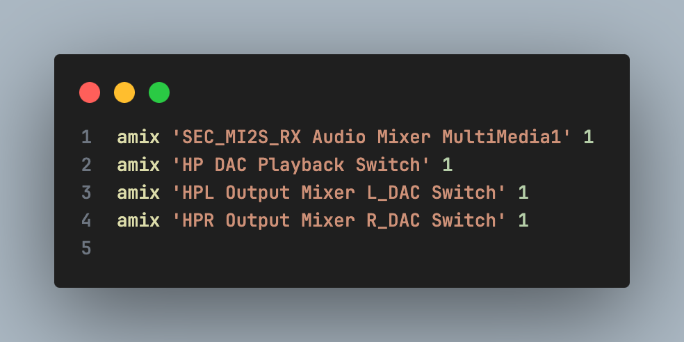
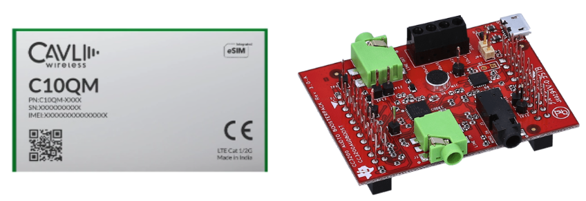
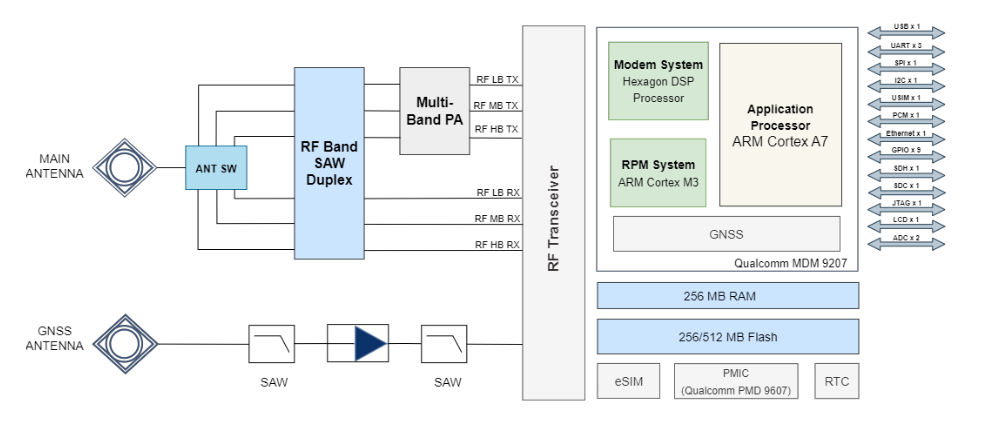
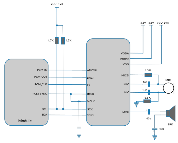
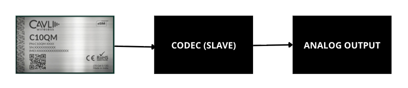 For downlink, audio data travels from the host device to the peripheral device. Specifically, digital PCM data is output by the C10QM module’s CPU via the PCM_DOUT pin (Pin 48). This signal enters the DIN pin of the TLV320AIC3254 codec. Here, the codec processes the signal through an interpolation filter and a digital-to-analog converter (DAC) to convert it into analog signal. The final signal is then passed through the amplifier (Headphone Driver) and output to the 3.5mm jack. Software-wise, the DAPM (Dynamic Audio Power Management) path is routed from the “Left/Right DAC” through the corresponding mixers to the HPL/HPR output.
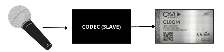 In contrast to the transmission stream, the uplink stream is responsible for bringing the signal from the environment into the processing system. The analog signal from the microphone enters the analog input of the codec, is amplified by the PGA (Programmable Gain Amplifier), and converted to digital via the ADC. The digital data is then output from the DOUT pin of the codec and goes to the PCM_DIN pin (Pin 47) of the C10QM module. At the C10QM side, the CPU receives this data stream to perform recording or processing for voice calls.
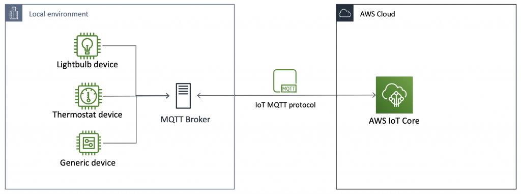

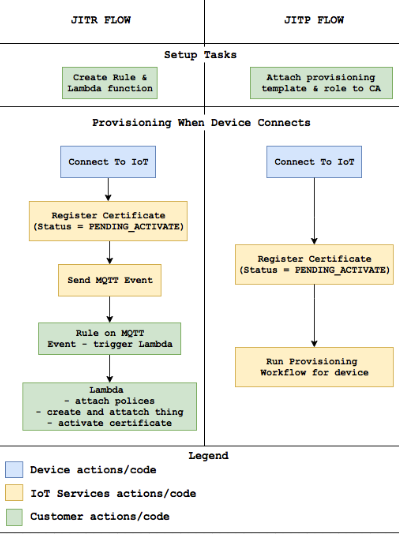
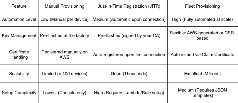
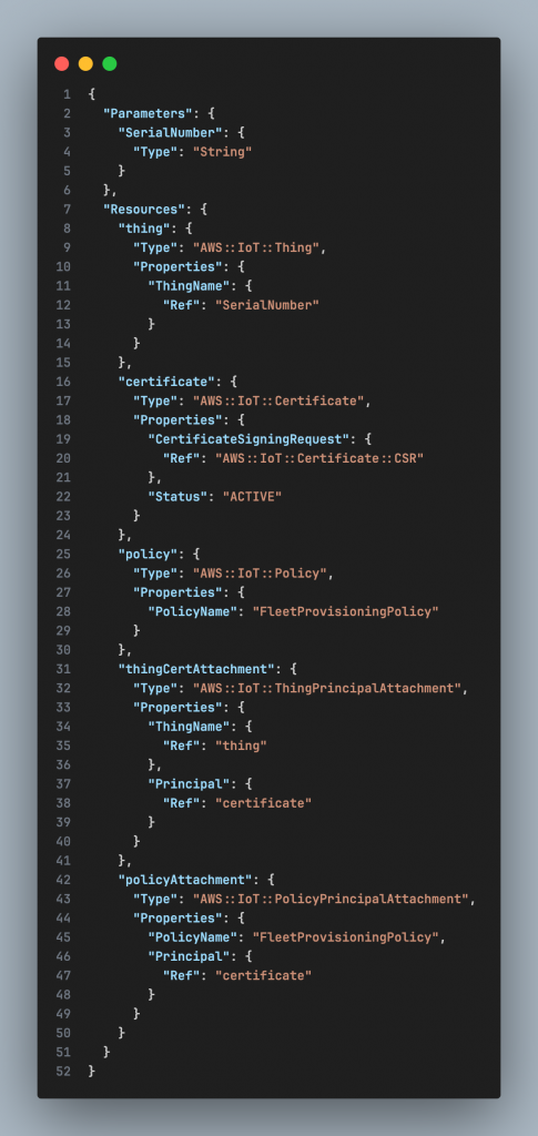
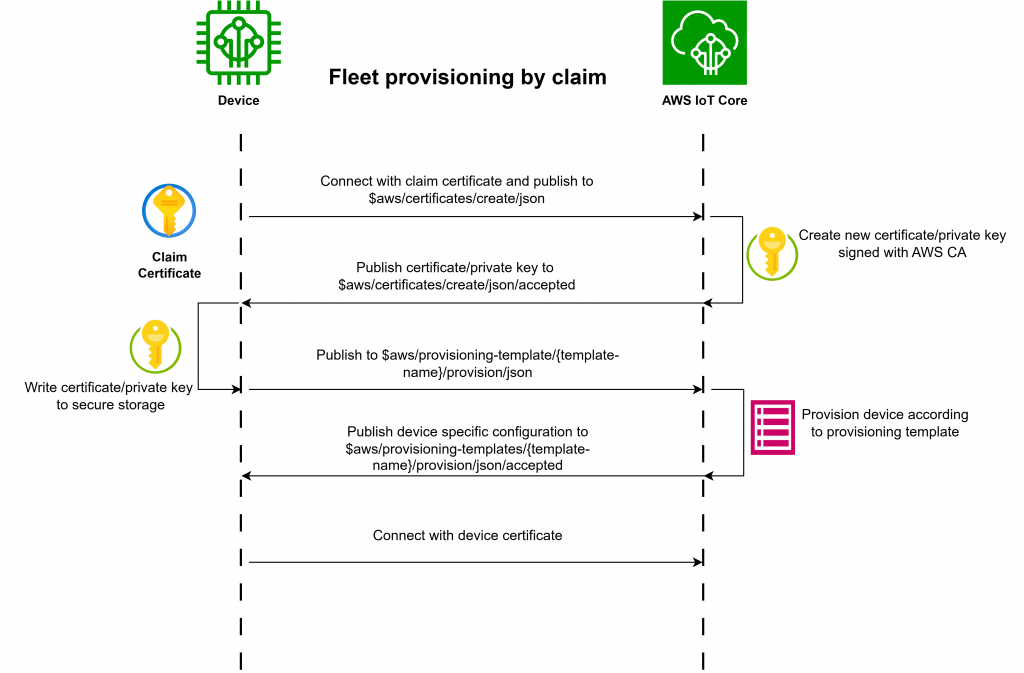
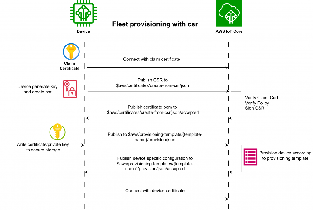
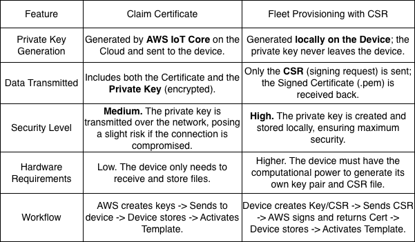
Fleet Provisioning provides a powerful mechanism that simplifies and fully automates the onboarding of devices into AWS IoT. By separating the identity provisioning process from firmware and delegating much of the certificate management responsibility to AWS, Fleet Provisioning allows systems to easily scale up while maintaining high security and efficient device lifecycle management.
Thanks to these features, Fleet Provisioning is particularly well-suited for mass-produced IoT systems, including cellular devices, gateways, and Wi-Fi, where rapid deployment, cost optimization, and long-term operational stability are required. In the context of modern commercial IoT, Fleet Provisioning is not just a technical choice, but a best practice for large-scale AWS IoT systems.

