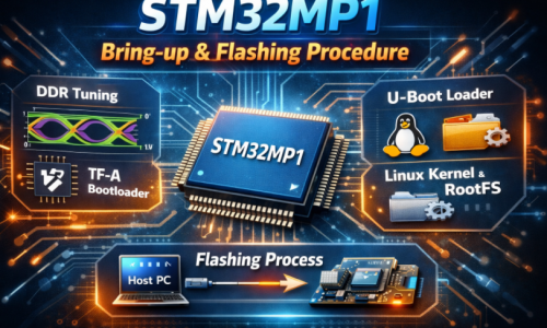
Why can’t the STM32MP1 boot from NAND Flash?
1. Layered Boot Chain Mechanism and the Role of ROM Code
1.1. Consistency of STM32 Image Header & Magic Number
1.2. Handshaking Protocol Between FMC and NAND (ONFI Compliance)
1.3. Bad Block Management (BBM) Mechanism
2. Check the Boot Pins (Hardware Strapping) configuration
2.1. Lookup table for Boot Mode STM32MP1.
2.2. How to check the voltage at the BOOT pin[2:0].
3. Compatibility Between ROM Code and ONFI Standard
3.1. How to Determine if a NAND Chip Supports ONFI
3.2. Handling Bus Width Errors (8-bit vs 16-bit) in Hardware
4. File Formatting Errors: The Importance of the STM32 Header
5. Configuring the Device Tree (DTS) for FMC and NAND
5.1. Setting the standard nand-ecc-mode and nand-ecc-strength according to the Datasheet
5.2. Optimizing FMC Clock Speed to Avoid Data Corruption
6. Analyzing Error Codes via UART Console
6.1.Connecting UART4 for ROM Code Debugging
6.2. Decoding Common Boot Failure Hex Codes
7. Checking for Bad Blocks and Flash Layout
7.1. Redundancy of FSBL on NAND
7.2. How to reload Flash Layout using STM32CubeProgrammer via DFU mode
Summary of the Quick Troubleshooting Checklist
Why can’t the STM32MP1 boot from NAND Flash?
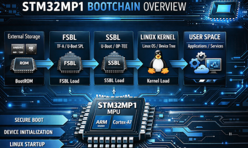
To fix the “Silent Boot” error (no console response), we need to delve into the boot chain mechanism of the STM32MP1 system. This process is not simply about reading data; it’s a coordinated sequence between hardware (FMC) and a tightly structured data set defined by the ROM code.
1. Layered Boot Chain Mechanism and the Role of ROM Code
When the system exits the Reset state, the first program to launch is Internal ROM Code. This is immutable source code embedded in the SoC. Its core task is to initialize the FMC (Flexible Memory Controller) to locate and load the FSBL (First Stage Boot Loader) — typically TF-A (Trusted Firmware-A) or U-Boot SPL — into the internal RAM (SYSRAM).
Problems often occur when the authentication chain or data loading process is interrupted at one of the following links:
1.1. Consistency of STM32 Image Header & Magic Number
ROM Code is an extremely strict state machine. It does not execute raw binary files (.bin) because it cannot determine the entry point and data integrity.
- Header Structure (256-byte): Contains important metadata including Image Length, Payload Checksum, and EntryPoint Address (the jump address in SYSRAM).
- Magic Number Identifier: ROM Code scans the blocks to find the code 0x324D5453 (equivalent to the ASCII string “STM3”).
- Consequential Error: If the loaded file is missing this header or the header is offset, ROM Code will return the error “No valid boot device found”. This is why you must use a .stm32 file (processed using mkimage or STM32CubeProgrammer).
1.2. Handshaking Protocol Between FMC and NAND (ONFI Compliance)
Physical layer errors are often caused by incompatibility between the FMC (Flexible Memory Controller) and the memory chip.
- Automatic ONFI detection: The STM32MP1 prioritizes the ONFI (Open NAND Flash Interface) standard for querying operating parameters such as page size, block size, and spare area size. Non-ONFI risk: If the NAND chip does not support ONFI, the ROM code is forced to use default parameters (FMC default timings). If there is a discrepancy in bus width (8-bit vs 16-bit), the read data will be corrupted.
- ECC Mismatch mechanism: This is the “silent killer.” The STM32MP1 uses hardware ECC (BCH4 or BCH8). Configuration error: If the programmer writes data using an ECC algorithm different from the algorithm the ROM Code uses for reading, the checksum will fail and the First Stage Boot Loader (FSBL) will be immediately aborted.
1.3. Bad Block Management (BBM) Mechanism
Unlike stable storage media such as SD Cards or eMMCs, NAND Flash allows for the existence of physical errors (Bad Blocks).
- Redundancy Scan: The ROM Code STM32MP1 will scan at least the first 128 KB to find valid headers.
- Skip-Block Mechanism: When encountering a Factory Bad Block (marked by the manufacturer), the ROM Code will automatically skip it and jump to the next block in the redundancy list.
- Programming Tool Logic Errors: A common technical error is that the programming tool fails to recognize the Bad Block or programs the wrong offset relative to the partition table (Flash Layout). If the FSBL is overwritten on a faulty block without being remapped, the ROM Code will be unable to initialize the Boot Chain.
2. Check the Boot Pins (Hardware Strapping) configuration.
2.1. Lookup table for Boot Mode STM32MP1.
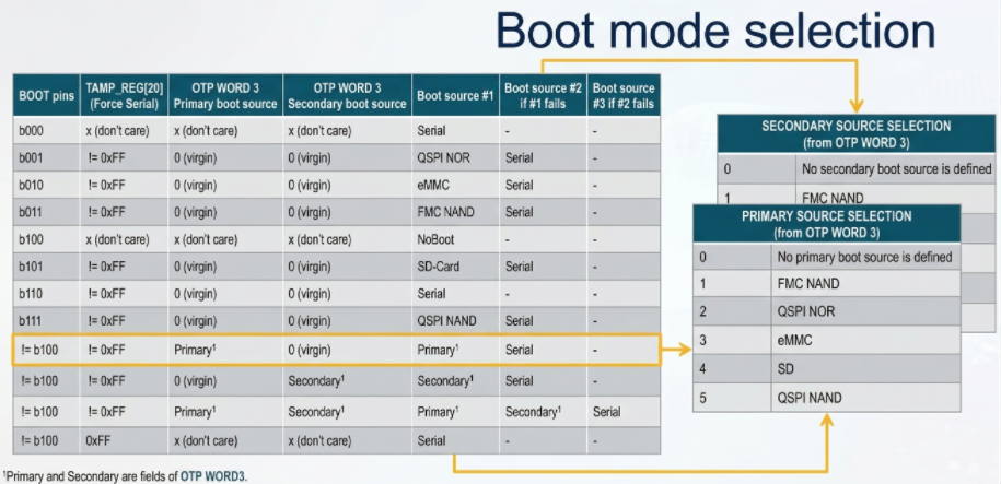
The STM32MP1 boot mode is defined by the combination of several inputs:
- Three boot pins, accessible on ST boards: their possible values are shown in the first column of the table;
- The next column corresponds to the TAMP backup register number 20, that allows the user to force a serial boot when it is set to 0xFF from U-Boot or Linux;
- The one time programmable WORD 3 contains a primary boot source and a secondary boot source, shown in the third and fourth columns, respectively. The possible values for the boot sources are listed in the tables on the right: parallel NAND Flash, QUADSPI NOR Flash, eMMC, SD Card or QUADSPI NAND flash.
The boot pins have two special positions:
- All pins at zero forces a boot in serial mode
- Binary value 100 allows to enter in no boot mode, useful to take the hand on the coprocessor via JTAG for 7 firmware development without Linux.
2.2. How to check the voltage at the BOOT pin[2:0].
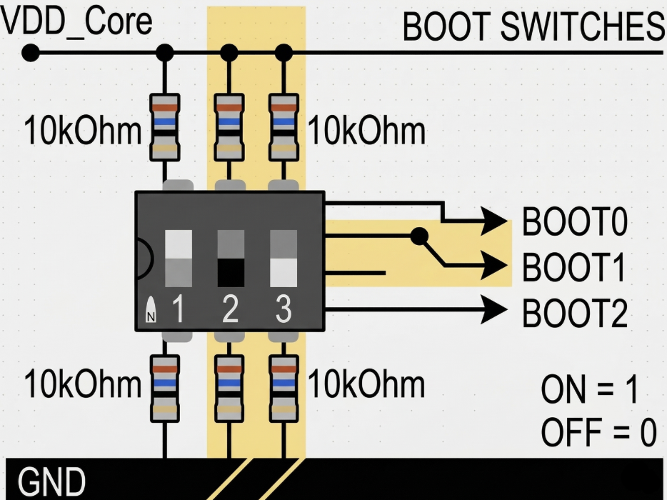
Configure Hardware Strapping using a 10kOhm resistor and Dip-Switch to select the boot source (NAND/SD/USB).
Sometimes flipping a switch or soldering resistors doesn’t guarantee the correct logic level due to noise or voltage drop. For accurate debugging, you need to follow these steps:
- Static Voltage Check: Use a multimeter to measure the voltage directly at the test points of the BOOT0, BOOT1, and BOOT2 pins while the board is powered on. High level ≥ 0.7 VDD vs Low level ≤ 0.3 VDD.
- Check for interference (Oscilloscope): The ROM Code only latches the values of the BOOT pins at the rising edge of the NRST signal. If the power supply is slow or the BOOT pin has an excessively large filter capacitor causing delay, the ROM Code may read an incorrect value. Use an oscilloscope to ensure the logic level is stable before releasing NRST.
- Determine the pull-up/pull-down resistance: If you are using resistors to fix logic levels, ensure the resistance value is between 10kΩ and 47kΩ. Avoid using excessively high values (such as 100kΩ) as this can cause logic level deviations due to I/O leakage current.
3. Compatibility Between ROM Code and ONFI Standard
One of the common reasons why the STM32MP1 cannot boot from NAND is the language difference between the ROM code and the flash chip. Unlike older microcontrollers that require hardcoded NAND parameters, the STM32MP1 prioritizes the use of an auto-recognition protocol.
3.1. How to Determine if a NAND Chip Supports ONFI
ONFI (Open NAND Flash Interface) is a standard that allows SoCs to query the technical specifications of NAND chips (such as block count, page size, spare area length) via the 0xEC command.
- Check the datasheet: Search for the keyword “ONFI” in the NAND chip’s technical documentation. Popular chip lines from Micron, Winbond, or Macronix usually support this standard.
- How does the ROM Code handle this?
During boot-up, the ROM Code sends the Read ID (0x90) and Read Parameter Page (0xEC) commands.
If the chip responds with the string “O-N-F-I”, the ROM Code will automatically configure the appropriate FMC controller for that chip.
- If the NAND does not support ONFI (Non-ONFI): The ROM Code will try based on the static ID table (Hardcoded IDs). If your chip is too new or too specific and not on ST’s supported list, the ROM Code won’t know how to read the data, leading to an immediate freeze.
3.2. Handling Bus Width Errors (8-bit vs 16-bit) in Hardware
Discrepancies in data bus width cause Data Mismatch errors, leading the ROM Code to incorrectly read the Bootloader Header.
- STM32MP1 Default: ROM Code initializes the FMC controller in 8-bit mode for backward compatibility.
- Using 16-bit NAND: If you are using a 16-bit NAND chip, the FMC_NIORDY pin (or some specific pin configuration) must be handled correctly. Most importantly, the STM32MP1 ROM Code only supports booting from 8-bit NAND. If your hardware design uses a 16-bit bus for the Boot partition, the system will not be able to boot (unless the NAND chip has an automatic 8-bit switching mode upon receiving a command).
- Physical connection check: Ensure that the signal lines from FMC_D0 to FMC_D7 are not short-circuited or open-circuited. Transmission impedance: With high access speeds, the data bus lines need to be of similar length to avoid signal skew.
4. File Formatting Errors: The Importance of the STM32 Header
A common mistake made by engineers new to the STM32MP1 family is directly loading raw binary files (.bin) onto NAND Flash. In reality, the STM32MP1’s ROM code doesn’t automatically understand where the binary file starts. It requires a technical “wrapper” surrounding the actual data, called the STM32 Image Header. If the loaded file lacks this header, the system will treat it as garbage and completely ignore it.
What is Magic Number 0x324D5453 Structure?
Each boot file (TF-A, U-Boot SPL) loaded onto NAND must begin with a 256-byte header. The most important component in this header is the Magic Number.
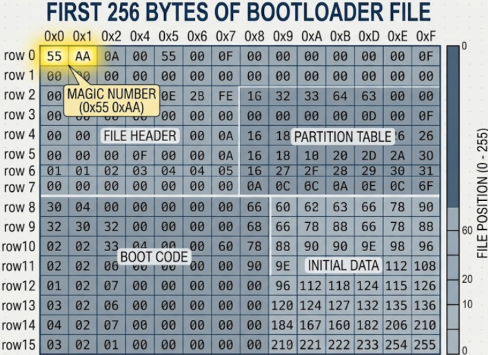
- Value: 0x324D5453 (When read in Little-endian format, it corresponds to the ASCII character string: “S-T-M-3”).
- Role: This is the “key” to unlock the ROM Code. When scanning through the Blocks on the NAND, the ROM Code only searches for this number. If the first 4 bytes of the Block do not match 0x324D5453, the ROM Code will immediately jump to the next Block.
- Other components in the Header: Image Signature, Image Length, Entry Point
When you compile with Yocto or Buildroot, the script will call the mkimage tool to package the u-boot-spl.bin file into u-boot-spl.stm32. This .stm32 extension is the indicator that the Header has been inserted. Otherwise you can use STM32CubeProgrammer to check Header:
- You can open the .stm32 file using Hex Editor software (such as HxD). If you see the first 4 bytes as 53 4D 54 32 (corresponding to “STM3”), your file has a standard header.
- When you connect the board in USB DFU mode, load the file into the corresponding partition: If you select a file without a header, the tool will immediately warn of a formatting error or the boot process will fail with the error log: “Header Not Found”. Using Flash Layout: The .tsv (Flash Layout) file in STM32CubeProgrammer will define partitions such as fsbl1, fsbl2. This tool automatically checks the integrity of the header before pushing data to the NAND.
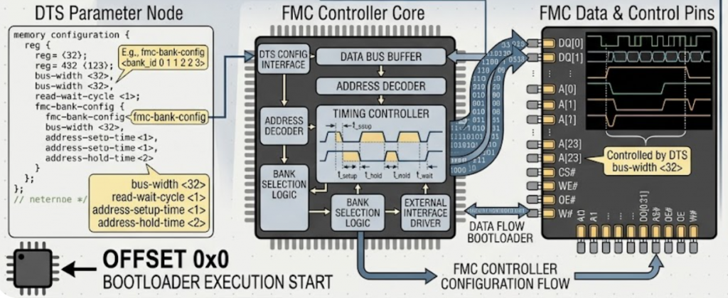
5. Configuring the Device Tree (DTS) for FMC and NAND
After the ROM Code has successfully loaded the FSBL, the next stage (U-Boot and Kernel) depends entirely on the data structure in the Device Tree (.dts). If the parameters here do not match the physical characteristics of the NAND chip, the system will freeze when trying to mount the data partition or report an “ECC uncorrectable error”.
5.1. Setting the standard nand-ecc-mode and nand-ecc-strength according to the Datasheet
To ensure data integrity, you need to open the datasheet of your NAND chip and find the “ECC Requirement” section.
- nand-ecc-mode: For STM32MP1, this value is usually “hw” (using hardware FMC acceleration). If your NAND chip has built-in error correction, use “on-die”.
- nand-ecc-strength: The number of error bits the controller is capable of correcting per data area (Step size).
Example: If the datasheet requires “8-bit ECC per 512 bytes”, set nand-ecc-strength = <8>. Note: STM32MP1 supports different strength levels (BCH4, BCH8). If the NAND chip requires 8-bit and you only configure 4-bit, the system will run unstably and quickly suffer from file corruption.
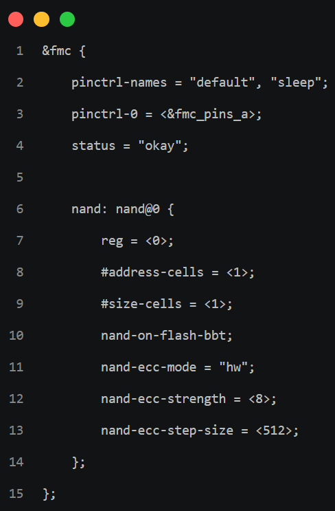
Mẫu cấu hình Device Tree chuẩn
5.2. Optimizing FMC Clock Speed to Avoid Data Corruption
Excessively high FMC control clock speeds cause random bit flips. The FMC controller must be configured with timings that match the NAND chip’s access speed.
- EBI Timings: Parameters such as tset, twait, and hold in the Device Tree define the minimum time for the data signal to stabilize before processing by the chip.
- Check Clock Speed: If you see many unidentified read errors in the U-Boot log, try reducing the FMC bus clock speed by adjusting it in the st,fmc-control button or reconfiguring the Clock Tree in the system’s .dts file.
6. Analyzing Error Codes via UART Console
When your STM32MP1 remains silent, the Internal ROM Code provides a “last-resort” diagnostic tool. Even before the first line of your code executes, the ROM Code can output specific error status characters to help you pinpoint exactly where the boot process failed.
6.1.Connecting UART4 for ROM Code Debugging
In STMicroelectronics reference designs (such as the Discovery or Eval boards), UART4 is the dedicated default console for ROM Code and bootloader debugging.
Default Pin Assignment:
- UART4_TX: Pin PG11 (Usually routed through an onboard ST-LINK or USB-to-UART bridge).
- UART4_RX: Pin PB2.
Terminal Configuration:
- Baud rate: 115200
- Data bits: 8
- Parity: None
- Stop bits: 1
- Flow Control: None
6.2. Decoding Common Boot Failure Hex Codes
If the NAND boot fails, the ROM Code emits an error character as defined in the AN5031 technical application note. Below is a breakdown of the most common codes encountered during NAND debugging:
| Hex Code | Technical Meaning (Error Meaning) | Troubleshooting / Solution |
|---|---|---|
| 0x61 | No Valid Header Found | The ROM Code scanned the entire NAND but did not find the Magic Number 0x324D5453. Check the .stm32 header file again. |
| 0x62 | Invalid Image Checksum | The header was found, but the internal data is corrupted or the ECC does not match. Verify the ECC configuration used during flashing. |
| 0x63 | Device Timeout / Not Ready | The NAND chip does not respond to read commands. Check the power supply (1.8V/3.3V) and the Ready/Busy (R/B) pin. |
| 0x64 | NAND ID Not Supported | The ROM Code can read the chip ID but does not support it (usually because it is not ONFI compliant). |
| 0x65 | Authentication Failed | This occurs when Secure Boot is enabled but the digital signature is invalid. |
7. Checking for Bad Blocks and Flash Layout
Unlike other memory types such as eMMC or SD Card, NAND Flash always comes with faulty blocks (bad blocks) from the factory. If the FSBL (TF-A) accidentally lands on a bad block without a redundancy mechanism, the STM32MP1 will never boot.
7.1. Redundancy of FSBL on NAND
The ROM code of the STM32MP1 is extremely intelligently designed to deal with bad blocks through a redundancy mechanism.
- FSBL Mirroring: Typically, we don’t just load a single FSBL. The system usually requires at least 2 to 5 copies of the FSBL (denoted as fsbl1, fsbl2, fsbl3…) located in the first blocks of the NAND.
- ROM Code Scanning Mechanism: 1. ROM Code starts scanning from Block 0. 2. If Block 0 is corrupted or lacks a valid STM32 header, it automatically jumps to the next block (usually Block 1 or the next offset depending on the configuration). 3. This process repeats until a complete FSBL is found.
- Offset Location: Typically, FSBLs are located at fixed positions (e.g., 0x00000000, 0x00040000, 0x00080000…). If you only load an fsbl1 into Block 0 and that block fails, the system will freeze.
7.2. How to reload Flash Layout using STM32CubeProgrammer via DFU mode
When NAND boot fails completely, the most thorough solution is to reload the entire partition structure via USB DFU (Device Firmware Update) mode.
Step 1: Firstly, switch to Serial Boot mode
Set the BOOT pins to level 000 (as instructed in section 1) and connect the board to the computer via USB OTG port.
Step 2: Next, prepare the Flash Layout file (.tsv)
The .tsv file is a “map” defining the location of each component on the NAND. A standard NAND file usually looks like this:
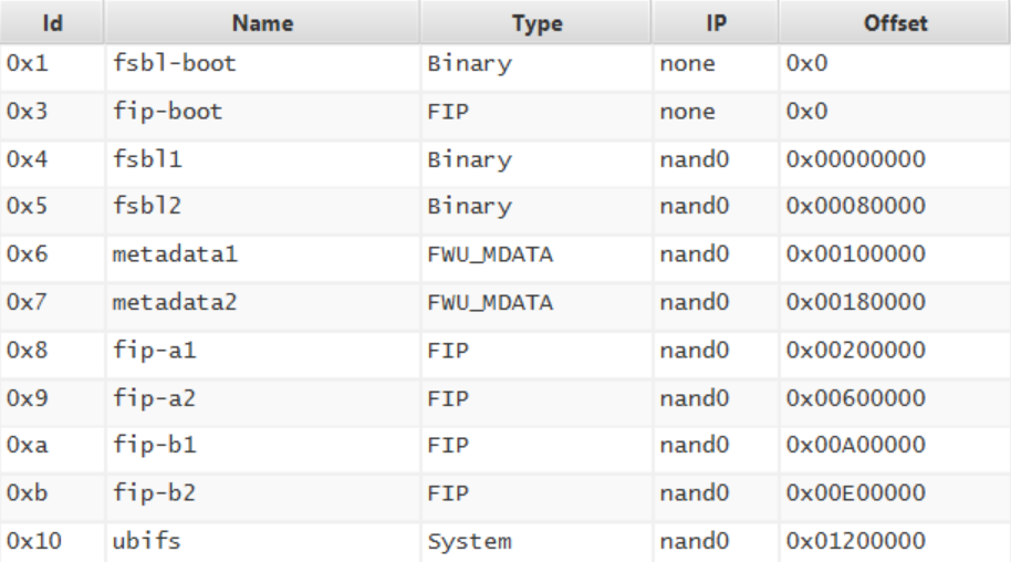
Note: The Offset column must match the Erase Size architecture of the NAND chip you are using.
Step 3: Finally, flashing the file
- Open STM32CubeProgrammer.
- Select the USB connection and click Connect.
- Switch to the Erasing & Programming tab and select the prepared .tsv file.
- Click Download.
- The tool will automatically remove bad blocks, calculate ECC values, and flash headers for each partition.
- If you encounter a Partition overlap error, check the file size against the offset.
Summary of the Quick Troubleshooting Checklist
| Category | Checklist Item | Status | Technical Notes |
|---|---|---|---|
| 1. Hardware | Boot Pins Strapping | [ ] | Ensure BOOT[2:0] = 010 (NAND Boot mode). |
| Voltage Levels | [ ] | Measure BOOT pins: High ≥ 0.7 VDD, Low ≤ 0.3 VDD. | |
| Bus Width | [ ] | ROM Code supports 8-bit NAND by default. | |
| Ready/Busy (R/B) | [ ] | Check pull-up resistor and connection to the SoC. | |
| 2. Image Header | Magic Number | [ ] | The first 4 bytes of the file must be 53 4D 54 32 (“STM3”). |
| File Extension | [ ] | Use .stm32 file, not a raw .bin file. | |
| Entry Point | [ ] | Must match the mapped address in SYSRAM. | |
| 3. NAND & ECC | ONFI Support | [ ] | Confirm the NAND supports ONFI or is in ST’s supported list. |
| ECC Strength | [ ] | Match nand-ecc-strength in DTS with the datasheet (4-bit / 8-bit). | |
| ECC Mode | [ ] | If using On-die ECC, disable FMC Hardware ECC. | |
| 4. Software / DTS | FSBL Redundancy | [ ] | Flash at least two copies (fsbl1, fsbl2) at the correct offsets. |
| TSV Partition | [ ] | Check the .tsv file to ensure no partition overlap. | |
| FMC Timings | [ ] | Increase tset and twait in DTS if random data errors occur. | |
| 5. Diagnostics | UART4 Log | [ ] | 115200, 8N1. Check Hex error codes (0x61, 0x62, 0x63). |
| USB DFU Mode | [ ] | Set BOOT to 000 to test connection via STM32CubeProg. |
📞 Technical Support & Consulting
Struggling with complex timing issues or custom hardware integration? We are here to help you accelerate your time-to-market.
Contact our embedded engineers at IES (Industrial Embedded Solutions) with email address [email protected] for expert hardware design review, custom bootloader development, and Linux kernel optimization.