NB-IoT: Principles and Architecture
1.What is NB-IoT? – Overview of Narrowband IoT
2. NB-IoT Network Architecture
2.1. LTE Access Network (eNodeB & Uu Interface)
2.2. Core Network (MME, SGW, PGW)
2.3. SCEF and Control Plane vs User Plane
3. NB-IoT Deployment Modes
4. NB-IoT Protocol Stack & Key Technologies
4.1. Physical Layer & Key Technologies
4.2. Power Saving Mechanisms: PSM & eDRX
4.3. Data Delivery: IP vs NIDD
5. Advantages and Limitations
6. NB-IoT Applications
7. Comparison with Other
1. What is NB-IoT? – Overview of Narrowband IoT
In recent years, the rapid development of the Internet of Things (IoT) has created an urgent need for communication technologies capable of connecting large numbers of devices with low power consumption and optimal operating costs. In this context, Narrowband Internet of Things (NB-IoT), standardized by 3GPP as an LPWAN technology operating on LTE mobile network infrastructure, targets IoT applications that do not require high data speeds but need reliability and long uptime.
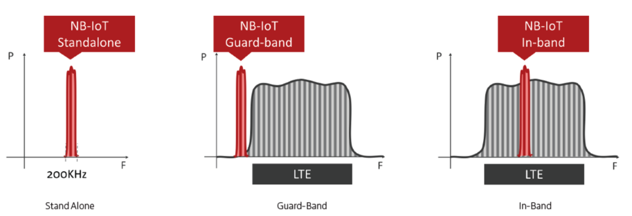
NB-IoT is a Radio Access Technology (RAT) directly integrated into the LTE ecosystem, leveraging eNodeB base stations, the core network, and existing LTE security mechanisms. This technology can be deployed in three models: in-band, guard-band, and standalone, but in all cases utilizes a narrow 180 kHz bandwidth to optimize spectrum efficiency and reduce the transmission power of the end device.
One of the most important characteristics of NB-IoT is its coverage enhancement capability. Thanks to its narrow bandwidth, high power density, and transmission loop mechanism, NB-IoT achieves a Maximum Coupling Loss (MCL) of up to approximately 164 dB, allowing for good signal penetration in environments with high signal attenuation such as basements, concrete structures, or high-density urban areas. This characteristic makes NB-IoT particularly suitable for static IoT applications, large-scale deployments, and applications requiring stable connectivity over extended periods, even in locations where traditional mobile technologies struggle.
 Furthermore, NB-IoT’s coverage is expanded by supporting low but stable uplink power, combined with optimized modulation and encoding for channels with high attenuation. This allows an NB-IoT base station to serve devices at the cell edge or in noisy environments while maintaining reliable communication. As a result, NB-IoT effectively meets the needs of deployment scenarios in hard-to-reach or inconvenient locations for maintenance, contributing to reduced operating costs and increased IoT system lifespan.
2. NB-IoT connection process
nb-iot structure
The Narrowband Internet of Things (NB-IoT) network architecture is a technical standard designed to connect a large number of smart devices with low power consumption and wide coverage. The core components of the system include:
- NB-IoT Devices: These devices are typically smart sensors or metering devices (such as water or electricity meters) that support NB-IoT technology.
- Electromagnetic Access Network (eNodeB): LTE base stations act as a wireless communication bridge between the devices and the core network.
- Evolved Packet Core (EPC): This is the central hub where data packets are processed, subscribers are managed, and packet switching services are performed.
- IoT Platform/Application Server: The endpoint where data is collected, analyzed, and services are provided to end users over the Internet.
NB-IoT systems have a distinct separation in how they handle communication protocols: First, non-IP transmission, meaning data from devices to the core network can be sent in raw form (NIDD – Non-IP Data Delivery) to optimize battery life and reduce device complexity. Second, with IP transmission, where data undergoes packet conversion (IP Packet Conversion) at the core network to ensure compatibility and transmission over standard internet environments. With this architecture, NB-IoT comprehensively ensures secure end-to-end communication from devices to application platforms; wide coverage with good penetration through walls and deep underground, suitable for urban or industrial environments; and large-scale connectivity leading to EPC core network systems designed to manage thousands of simultaneous connections across multiple sectors such as Smart Cities, Logistics, and Energy.
Based on the NB-IoT network architecture, we will delve into the details of the core technical components that enable this system to operate stably and securely. From wireless connectivity at the base station to data processing at the core network, each component plays a specialized role:
2.1. LTE Access Network (eNodeB & Uu Interface)
This is the first receiving layer in the model, responsible for establishing a physical connection with the device:
- eNodeB (LTE Base Station): These are improved base stations based on the traditional LTE standard, optimized for NB-IoT. They manage radio signal transmission and reception, coordinate resources, and ensure wide coverage for thousands of devices in an area.
- Uu Interface: This is the wireless connection interface between the device (UE) and the eNodeB. In NB-IoT, this interface is optimized to transmit small packets with extremely narrow bandwidth (Narrowband), minimizing interference and saving energy for the end device.
For example, this diagram shows: eNodeB (evolved NodeB), which are base stations in an LTE/NB-IoT network. In the diagram, the stations are numbered eNodeB#1, #2, #3, forming the radio access network; MME/S-GW: These are entities belonging to the Core Network. The MME manages control, while the S-GW manages user data flow. The interfaces include: Uu interface (not directly displayed by labels but implicitly) is the wireless connection between the device (UE) and the eNodeB stations; X2 interface: Solid lines directly connecting the eNodeB stations to each other. This interface is extremely important for handover and interference reduction coordination between stations; S1 interface: This is a dashed line connecting each eNodeB to the MME/S-GW. It is divided into two types:
- S1-MME: Used for control signals (Control Plane).
- S1-U: Used for user data (User Plane).
The entire cluster of eNodeBs and the X2 connections between them are collectively called E-UTRAN (Evolved Universal Terrestrial Radio Access Network). This is the “Access Network” that allows IoT devices to access the telecommunications network.
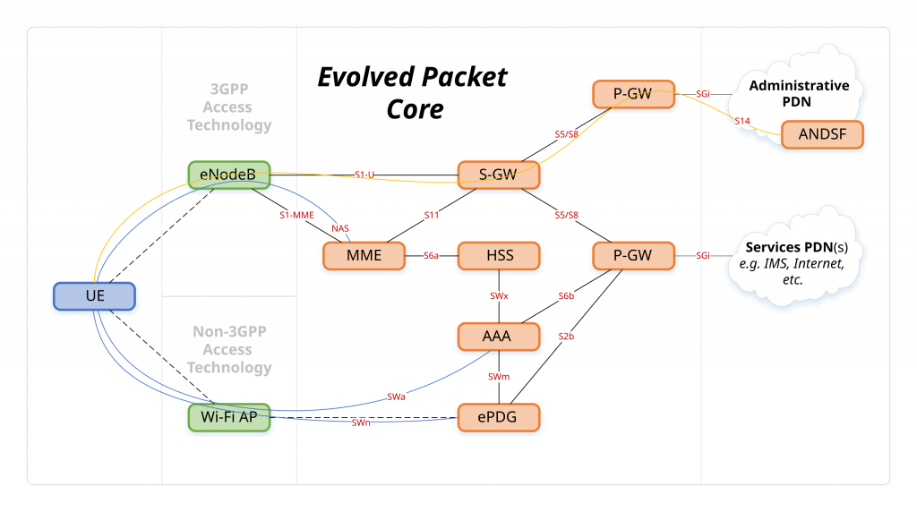
2.2. Core Network (MME, SGW, PGW)
The EPC (Evolved Packet Core) network acts as the “brain” coordinating the entire data flow:
- MME (Mobility Management Entity): Responsible for managing mobility, authenticating devices when joining the network, and selecting appropriate service gateways for data transmission.
- S-GW (Serving Gateway): Acts as a data forwarding anchor point between the wireless access network and the core network. It ensures that packets are correctly routed when devices move or change their connection state.
- P-GW (PDN Gateway): Is the final connection point of the core network to external networks (Internet/ISP). P-GW performs tasks such as assigning IP addresses to devices (in the case of using IP) and enforcing Quality of Service (QoS) policies.
2.3. SCEF and Control Plane vs User Plane
These are the key components that help differentiate efficient data transmission methods in NB-IoT:
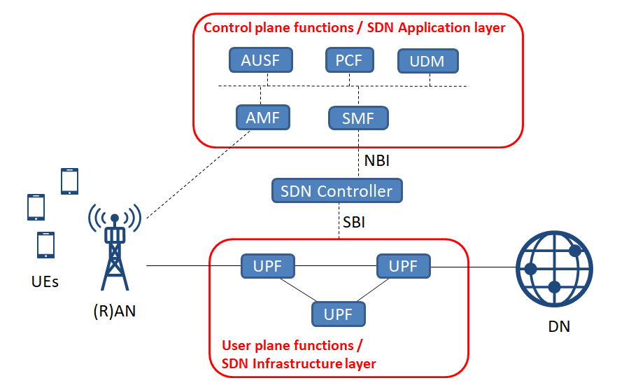
- SCEF (Service Capability Exposure Function): A specialized component for non-IP IoT devices. SCEF allows the core network to securely transmit small amounts of data through the control plane, eliminating the need for complex IP data session setups.
- Control Plane: Often used in NB-IoT to transmit even small application data (via NIDD). This is extremely efficient as it reduces redundant connection setup steps, maximizing battery life for sensors.
- User Plane: The traditional IP-based data transmission path (CIOT Data Plane). It is typically used for applications requiring larger data volumes or standard network protocols when connecting to IoT platforms.
The coordination between these layers creates an end-to-end secure communication cycle, ensuring that data from even the simplest sensors can be securely transmitted to the centralized management platform.
3. NB-IoT Deployment Modes
simulation nb-iot modes
The frequency spectrum of NB-IoT technology allows carriers to flexibly optimize their existing infrastructure: Standalone utilizes a separate frequency band, Guard-band exploits the guarded gaps between carriers, and In-band integrates directly into the existing LTE bandwidth. Each mode has different advantages and disadvantages; for easy comparison, the features are summarized in detail in the table below:
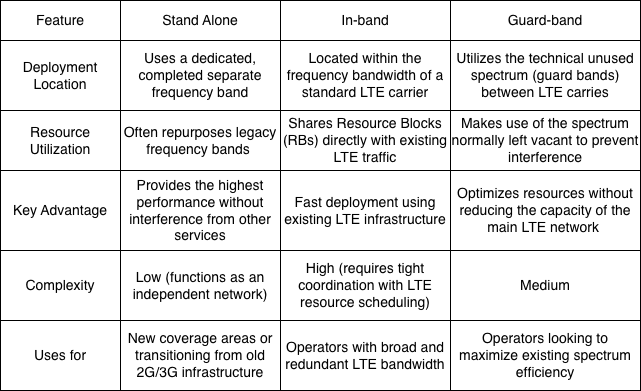
table of nb-iot’s feature
4. NB-IoT Protocol Stack & Key Technologies
nb-iot protocol stack
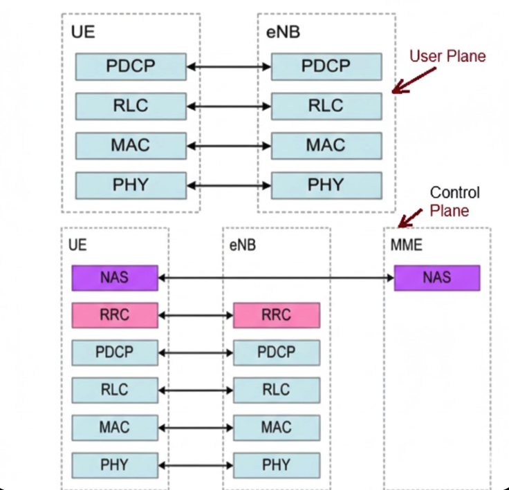
This diagram illustrates how data and control commands are packaged and transmitted across different layers in an NB-IoT system to ensure synchronization between devices and network infrastructure. In the User Plane, the plane responsible for transmitting the actual user data between the device (UE) and the base station (eNB) is involved. Protocol layers include: PDCP (Packet Data Convergence Protocol) for header compression/decompression and data security; RLC (Radio Link Control) for data segmentation, reassembly, and ARQ error control; MAC (Medium Access Control) for scheduling and coordinating channel access; and PHY (Physical Layer) for transmitting physical signals over the radio space. On the other hand, in the Control Plane, this plane manages network connections, signaling, and control, involving three entities: the UE, the eNB, and the core network (MME). The additional layers include: NAS (Non-Access Stratum), the highest layer, which directly communicates between the UE and MME to manage mobility, authentication, and session establishment; RRC (Radio Resource Control), which manages the radio connection state between the UE and eNB (establishing, configuring, maintaining, and releasing connections); and the lower layers (PDCP, RLC, MAC, PHY), similar to the user plane but used to transmit control information instead of user data.
4.1. Physical Layer & Bandwidth
The physical layer of NB-IoT is specifically designed to optimize cost, energy, and extreme penetration capabilities. The system operates on a total bandwidth of 200 kHz, but actually utilizes 180 kHz, equivalent to a Resource Block in LTE. In terms of multiple access techniques, the downlink uses OFDMA with a subcarrier spacing of 15 kHz, while the uplink uses SC-FDMA supporting both single-tone (3.75 kHz or 15 kHz) and multi-tone (15 kHz) transmission.
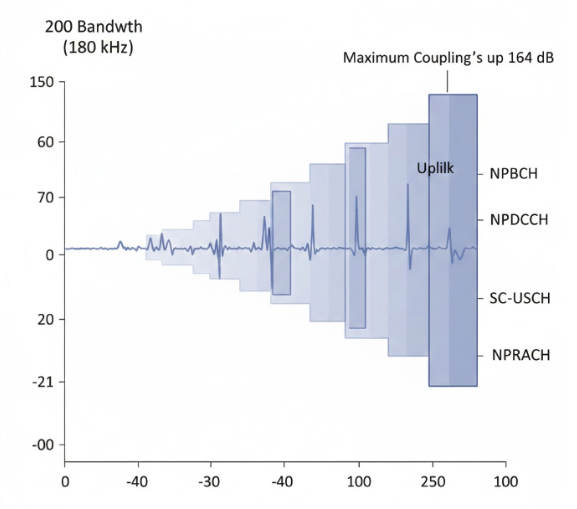
In particular, coverage is significantly improved thanks to a Maximum Coupling Loss (MCL) of up to 164 dB, combined with packet repetition techniques to ensure accurate transmission even in extremely weak signal conditions such as deep basements. This process is operated through a system of dedicated physical channels including NPBCH for system information transmission, NPDCCH for control and scheduling, NPDSCH and NPUSCH for user data transmission for downlink and uplink respectively, and NPRACH to support initial network access procedures.
4.2. Power Saving Mechanisms: PSM & eDRX
These are two key mechanisms that enable NB-IoT devices to extend battery life to over 10 years:
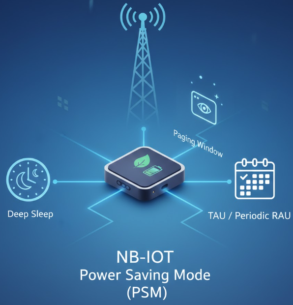
- PSM (Power Saving Mode): Allows the device to enter a deep sleep state while remaining registered with the network without needing to repeat complex connection procedures. In this mode, the device cannot be awakened by the network (Unreachable) until it actively sends data periodically.
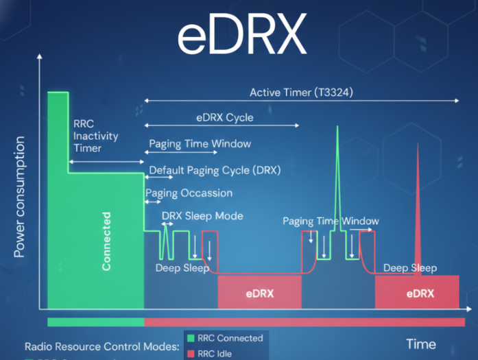
- eDRX (Extended Discontinuous Reception): Extends the signal checking cycle from the base station (Paging). Instead of continuous checking, the device only “wakes up” to listen for control signals during pre-configured intervals, significantly reducing power consumption compared to traditional DRX.
The core energy-saving mechanism of NB-IoT allows devices to operate for many years on a single battery. Below is a detailed description of the components in the diagram:
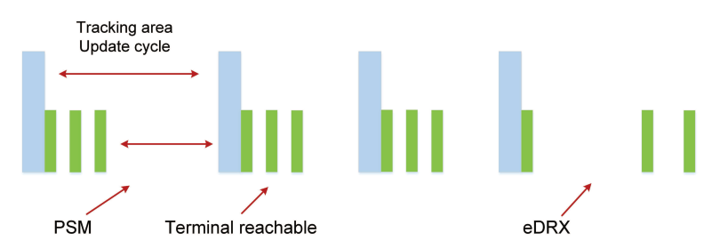
To optimize battery life for NB-IoT devices, the PSM and eDRX mechanisms play a key role in managing operating state and power consumption. PSM (Power Saving Mode) allows the device to enter a deep sleep state after completing the Tracking Area Update cycle, maximizing power savings because the device is completely unreachable from the network during this period. Meanwhile, eDRX (Extended Discontinuous Reception) extends the interval between device wake-ups for signal checking (paging), allowing the device to maintain a terminal reachable state more flexibly while significantly reducing power consumption compared to traditional check cycles. The seamless coordination between these two mechanisms helps the device balance data transmission and reception needs with the goal of extending battery life for decades.
4.3. Data Delivery: ID vs NIDD
NB-IoT offers two flexible data transmission methods depending on the application’s needs:
- IP Data Delivery (ID): Data is encapsulated using standard IP protocols (such as IPv4 or IPv6), suitable for applications requiring high compatibility with existing Internet platforms and the transmission of larger volumes of data.
- Non-IP Data Delivery (NIDD): Allows the transmission of raw data without the IP packet header; data is transmitted through the Control Plane via the SCEF entity, reducing packet size and maximizing battery life for the device. This is optimized for sensors sending extremely small data (a few tens of bytes) and enhances security because the device does not have a public IP address, helping to avoid common cyber attacks.
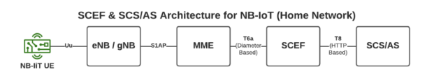 Unlike conventional IP data transmission (via SGW/PGW), this diagram accurately describes the NIDD route, enabling NB-IoT devices to maximize battery life and enhance security by not using public IP addresses. The presence of SCEF (Service Capability Exposure Function) is a core and unique component found only in the Non-IP data transmission route. It acts as a “gateway” to encapsulate raw data from the IoT device into control messages. Transmission via MME (Mobility Management Entity): In this diagram, data travels from eNB/gNB via the S1AP interface to the MME, then to the SCEF via the T6a interface. This route confirms that data is being transmitted on the Control Plane, a characteristic of the NIDD method for energy optimization. Connection to SCS/AS: After passing through the SCEF, data is transferred to the application platform (SCS/AS) via the T8 interface (based on HTTP). This is how devices without IP addresses can still communicate with servers on the Internet.
5. Advantages & Limitations
Advantages of NB-IoT
The main reasons for choosing NB-IoT connectivity, similar to LTE-M, include low power consumption, efficient spectrum utilization, and low deployment costs. These characteristics make NB-IoT particularly suitable for large-scale and long-term IoT systems.
Regarding power consumption, NB-IoT introduces two key power-saving mechanisms that give it an edge over older mobile networks like 2G, 3G, or 4G in IoT applications. Power Saving Mode (PSM) allows the device to enter a deep sleep state when not transmitting data, while maintaining its network subscription status. Unlike mobile phones – which need to maintain a constant connection to receive calls or messages – IoT devices typically transmit data only in defined cycles and require virtually no downlink. Therefore, they don’t need to send periodic Tracking Area Update (TAU) messages to inform the network of their location, significantly reducing power consumption. With PSM, the device can completely disconnect RF for extended periods without needing to repeat the attach procedure upon waking up.
For applications that still require network data reception capabilities, NB-IoT offers an Extended Discontinuous Reception (eDRX) mechanism. While conventional mobile devices must continuously check the radio channel in very short cycles, eDRX allows for extended paging listening periods of up to tens of minutes. This enables the device to still receive downlink messages such as configuration changes, firmware updates, or remote access, but with significantly lower power consumption compared to traditional DRX mechanisms.
NB-IoT is also designed to use spectrum efficiently. This technology operates on narrow bandwidths, reducing interference and enabling high device density deployment within the same cell. In addition to utilizing existing LTE bands, NB-IoT can also leverage guard bands – the portion of spectrum between LTE channels – to optimize radio resources. This approach allows carriers to expand the number of connected devices without significantly impacting the quality of service for traditional mobile users.
Indoor coverage, according to the Maximum Coupling Loss (MCL) index defined by 3GPP, NB-IoT achieves a theoretical MCL of up to 164 dB, higher than most other LPWAN technologies. This allows NB-IoT signals to penetrate thick building materials and operate stably in high-interference environments. However, to achieve this level of coverage, NB-IoT must use a packet repetition mechanism, leading to certain trade-offs in energy consumption.
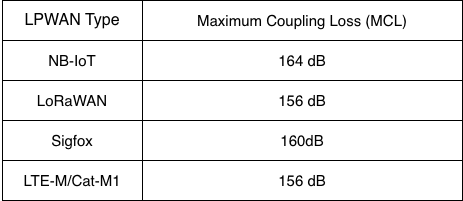
LIST OF MCL LPWAN
In terms of cost, NB-IoT uses modems with a simpler architecture compared to broadband LTE or 5G, thereby reducing hardware costs and total cost of ownership (TCO). NB-IoT modems have high global compatibility, facilitating multinational deployments. However, in some cases, NB-IoT devices need to support backup technologies such as 2G when NB-IoT coverage is not yet available, which can increase chipset complexity and cost.
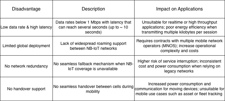
Limitations of NB-IoT
Despite its many advantages for static IoT applications, NB-IoT still has significant limitations, especially when compared to LTE-M, which need to be carefully considered before large-scale deployment.
6. Application of NB-IoT
NB-IoT is a LPWAN technology optimized for IoT scenarios with low data traffic, low transmission frequency, and long battery life requirements. By trading off speed, latency, and mobility, NB-IoT achieves deep coverage, high stability, and minimal power consumption. However, limitations in throughput, roaming, redundancy, and handover make NB-IoT unsuitable for real-time, mobile, or global deployments. Therefore, the selection of NB-IoT should be based on specific application characteristics, rather than viewing it as a universal IoT solution.
Thanks to its stable operation and energy efficiency, NB-IoT is particularly well-suited for large-scale, static IoT systems where each device transmits only a small amount of data over long cycles. Typical applications include smart metering (electricity, water, gas), environmental monitoring (air quality, water level, temperature), smart urban infrastructure (streetlights, parking lots), smart agriculture, and indoor or underground fixed asset tracking systems. In these scenarios, NB-IoT offers optimal efficiency in terms of operating costs, battery life, and long-term reliability.
7. Comparison between NB-IoT & LTE-M
NB-IoT and LTE-M are two LPWAN technologies developed by 3GPP to support large-scale IoT connectivity over mobile network infrastructure. In IoT systems, coverage plays a crucial role, especially for devices deployed indoors, underground, or at the cell edge.
NB-IoT is optimized for deep coverage thanks to its narrow 180 kHz bandwidth and transmission loop mechanism, achieving a Maximum Coupling Loss (MCL) of approximately 164 dB, suitable for static devices in environments with high signal loss. Meanwhile, LTE-M provides wider coverage with better mobile support, having an MCL of approximately 156 dB, suitable for both static and mobile scenarios.
Beyond coverage, the choice between NB-IoT and LTE-M also depends on factors such as speed and latency, mobility, power consumption, device cost, and roaming capabilities. These differences are summarized and compared in detail in following the table:
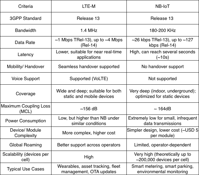
THE COMPARISON BETWEEN LTE-M VS NB-IOT
LTE-M is well suited for IoT applications that require mobility, lower latency, higher data rates, OTA firmware updates, voice support, and global roaming. NB-IoT is optimized for static IoT devices that transmit very small amounts of data, infrequently, and require deep coverage and multi-year battery life. Fundamentally, these two technologies do not directly compete, but rather complement each other within the Mobile IoT ecosystem.
CAN Bus Protocol
1. Introduction – CAN Protocol Overview
2. CAN Standard & ISO (11898-1, 11898-2, 11898-3)
3. Network Topology & Physical layer
4. CAN Frame Types
4.1. Data Frame
4.2. Remote Frame
4.3. Error Frame
4.4. Overload Frame
5. Message fields & Arbitration
6. Error detection & Bus fault handing
7. CAN FD Overview
8. Higher layer protocols on CAN
9. Application
9.1. CAN Bus (Classical CAN)
9.2. CAN FD (Flexible Data rate)
10. Conclusion
1. Introduction – CAN Protocol Overview
CAN (Control Area Network) is a highly reliable multipoint serial communication standard first developed by Robert Bosch GmbH, Germany, in 1986 when they were asked by Mercedes to develop a communication system between three ECUs (electronic control units) in a vehicle. Although UART (Universal asynchronous receiver-transmitter) is a widely used protocol, it does not adequately meet the requirements of multi-node systems, high-noise environments, and the demanding reliability requirements of the automotive industry. CAN was designed to address these limitations. The CAN bus operates effectively in high electromagnetic interference environments with twisted pair CAN High and CAN Low wires combined with fault checking and automatic fault detection mechanisms. Devices within the same bus are called nodes; a system can add several nodes, ranging from a few hundred to several kilometers, while still ensuring signal transmission. A key feature of CAN is its ID-based prioritization (arbitration) mechanism, which allows messages to be transmitted earlier without causing data conflicts. It offers high-speed transmission rates of up to 1 Mbits/second to enable time-based control.
Based on Bosch’s technical specifications, version 2.0 of CAN is divided into two parts:
- Standard CAN (Version 2.0A): uses an 11-bit ID (Identifier).
- Extended CAN (Version 2.0B): uses a 29-bit ID.
The two parts are defined by different message IDs, with the main difference being the length of the ID code. There are two ISO standards for CAN. The difference lies in the physical layer: ISO 11898 handles high-speed applications up to 1 Mbit/second, and ISO 11519 has an upper limit of 125 kbit/second; larger data sizes meet the needs of modern systems. Thanks to these advantages, CAN buses are widely used not only in automotive but also in industrial, medical, aerospace, and automation fields.
2. CAN Standards & ISO (11898-1, 11898-2, 11898-3)
OSI Layers
The OSI (Open Systems Interconnection) reference model, proposed by ISO, aims to standardize data communication processes in network systems. The OSI model comprises seven layers, each responsible for a distinct function, from physical signal transmission to application-level data processing, enabling different systems to communicate compatiblely and efficiently.
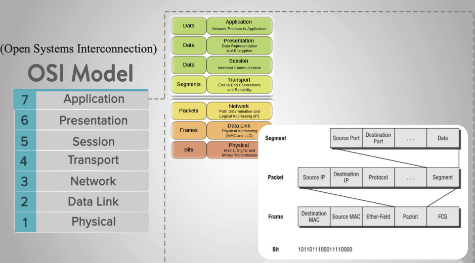
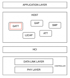
In practice, not all communication protocols fully implement all seven layers of the OSI model. For embedded systems and industrial control networks, especially in the automotive sector, protocol architectures are often simplified to reduce latency, increase reliability, and meet real-time requirements. A typical example is CAN Bus (Controller Area Network); a serial communication protocol designed for distributed control systems where multiple nodes need to exchange data with high reliability and fast response times. CAN does not fully implement all seven OSI layers, but mainly focuses on the two lowest layers:
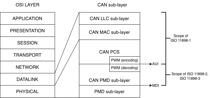
- Physical Layer: defines the transmission medium, voltage levels, connection methods, and signal characteristics.
- Data Link Layer: defines the transmission frame structure, bus access mechanism, error detection, and collision handling.
The remaining layers of the OSI model (Network, Transport, Application, etc.) are usually implemented through higher-layer protocols such as CANopen, J1939, or are defined by the manufacturer.
ISO 11898
To ensure the compatibility and stable operation of the CAN Bus in various environments, the CAN protocol has been standardized in the ISO 11898 standard. This standard details how CAN operates in relation to the layers of the OSI model, specifically:
- ISO 11898-1: Specifies the Data Link Layer and Physical Signalling mechanism of the CAN protocol, which serves as the core of the CAN Bus architecture. This standard details the structure of the CAN transmission frame, including Data Frame, Remote Frame, Error Frame, and Overload Frame, and defines the bus access mechanism through a contention process based on the priority level of the identifier (ID). In addition, ISO 11898-1 also specifies error detection and handling methods such as CRC, bit stuffing, ACK acknowledgment mechanism and error counters, as well as bit synchronization and data transmission timing techniques. This standard supports both standard CAN with 11-bit identifiers and extended CAN with 29-bit identifiers, ensuring reliable communication between nodes in a CAN network, avoiding data conflicts, and automatically detecting errors during transmission.
- ISO 11898-2 defines the Physical Layer for High-Speed CAN, commonly known as High-Speed CAN (HS-CAN), to meet the requirements of systems with high bandwidth and low latency. According to this standard, CAN can achieve transmission speeds up to 1 Mbps and uses differential twisted pair CAN_H and CAN_L to enhance noise immunity. The dominant and recessive states are distinguished by differential voltage levels, where CAN_H and CAN_L are approximately 3.5 V and 1.5 V respectively in the dominant state, and approximately 2.5 V in the recessive state. ISO 11898-2 requires the use of 120 Ω termination resistors at both ends of the bus to ensure signal quality, making this standard widely applied in critical control systems such as engine ECUs, ABS, ESP, and automotive drive and safety systems.
- ISO 11898-3: Describes the physical layer for low-speed, fault-tolerant CAN, also known as Low-Speed or Fault-Tolerant CAN, with the goal of maintaining system operation even in the event of a transmission failure. This standard supports a maximum transmission speed of 125 kbps and allows the CAN network to continue operating if one of the two transmission wires is broken. Unlike high-speed CAN, ISO 11898-3 does not require bus termination resistors and incorporates mechanisms for detecting and isolating faulty nodes to improve system reliability. Thanks to these characteristics, CAN according to ISO 11898-3 is often used in vehicle systems such as door, window, and light control, and applications that do not require high speed but need stability and safety in harsh working environments.
Thus, ISO 11898 serves as a bridge between the OSI model and the practical implementation of CAN Bus, helping to clearly define which layers CAN operates at and ensuring standardization in modern embedded systems and control networks.
3. Network Protocol & Physical layer
In a CAN Bus system, nodes are connected using a bus topology, where all devices share a common transmission line. Each node is connected in parallel to the bus via a pair of CAN_H and CAN_L wires, allowing multiple nodes to participate in communication without a central control device. This topology reduces the number of connecting wires, simplifies the system, and increases scalability. Bus access is controlled by non-destructive arbitration, ensuring that high-priority messages are transmitted first without losing data from other nodes.
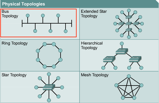
Bus Topology model
At the physical layer, the CAN Bus uses differential signaling via two lines, CAN_H and CAN_L, to enhance electromagnetic interference resistance. In the recessive state (logic ‘1’), the voltages on the CAN_H and CAN_L lines are approximately equal and usually around the common-mode voltage, around 2.5 V. When transmitting a dominant bit (logic ‘0’), the transmitter creates a voltage difference between the two lines, where CANH is pulled up to a higher voltage level and CAN_L is pulled down to a lower voltage level. The receiver does not rely on absolute voltage values but decodes data based on the differential voltage difference between CAN_H and CAN_L, helping the CAN system operate stably in high-noise environments such as automotive and industrial applications.
The figure below illustrates the principle of differential signal transmission and reception in the CAN Bus at the physical layer, showing the block structure of the CAN transmitter circuit, the CAN_H and CAN_L voltage waveforms corresponding to the dominant and recessive states on the bus, as well as the operating principle of the receiver circuit based on the differential voltage comparator. Through this mechanism, the CAN Bus ensures reliable information transmission while effectively supporting bus contention and error detection.
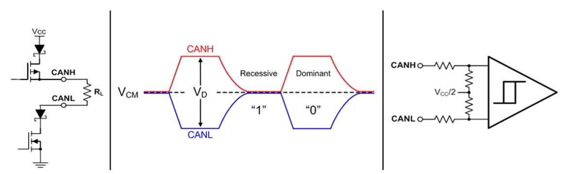
The principle of differential signal transmission and reception of the CAN Bus at the physical layer
Furthermore, to ensure signal quality during transmission, CAN Bus requires the use of termination resistors, typically 120 Ω, placed at both ends of the bus. These resistors reduce signal reflections and maintain stable transmission impedance. Bus length and transmission speed are inversely proportional; as transmission speed increases, the allowable bus length decreases. Thanks to the combination of a simple bus topology model and a physical layer using differential communication, CAN Bus achieves high reliability, good noise immunity, and is widely used in embedded systems, especially in the automotive field.
4. CAN Frame Types
4.1. Data Frame
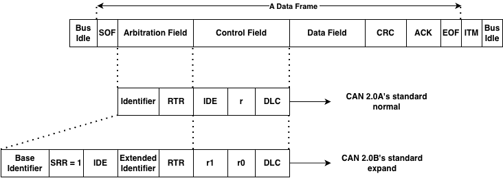
frame data of can
A CAN data frame is the basic communication unit on the CAN bus, used to exchange information between nodes in the system. A CAN frame begins and ends when the bus is idle, ensuring all nodes are ready for data transmission.
The data frame starts with the SOF (Start Of Frame) field, which includes a dominant bit used to synchronize all nodes on the bus and signal the start of a new data transmission session.
Next is the Arbitration Field, which determines the priority level of a message when multiple nodes are transmitting simultaneously. This field contains the Identifier (ID) and the RTR (Remote Transmission Request) bit. The illustration shows both CAN formats: standard with an 11-bit ID and extended with a 29-bit ID. In the arbitration mechanism, messages with smaller IDs have higher priority and are transmitted first without collisions.
Next is the Control Field, which includes bits identifying the frame type (IDE), reserve bits, and DLC (Data Length Code). The DLC indicates the number of bytes of data transmitted in the Data Field, up to 8 bytes for the CAN 2.0 standard.
The Data Field contains the actual information content of the message. Depending on the DLC value, this field can be from 0 to 8 bytes long. This is the main payload used by ECUs to exchange status, control commands, or sensor data.
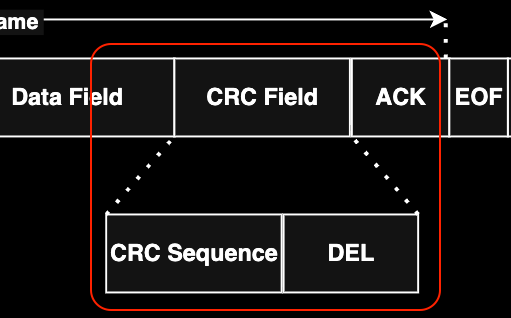
To ensure data integrity, the CAN frame includes a CRC Field, which contains the CRC error check code. The receiving node recalculates the CRC and compares it to the received CRC to detect errors during transmission.
Next is the ACK Field. If a node receives valid data, it pulls the bus down to the dominant level to send an acknowledgment signal. Failure to receive an ACK will cause the transmitting node to automatically retransmit the message.
The data frame ends with EOF (End Of Frame), a 7-bit recessive, marking the end of the transmission. This is followed by Intermission, a short pause required before any new CAN frames can be sent.
4.2. Remote Frame
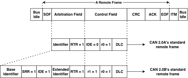
Besides Data Frames used for data transmission, Remote Frames are used to request data from any node on the same bus. However, remote frames are rarely used in automotive projects because data transmission is not request-based but primarily proactive, relying on information from the car’s specifications. Similar to Data Frames, the frame is clearly marked as a Remote Frame via the RTR bit, and this frame does not have a data field. Depending on the CAN network implementation, responses may be sent automatically. Simple CAN controllers (BasicCAN) cannot respond automatically. In this case, the Master microcontroller recognizes the remote request and must send data proactively.
4.3. Error Frame
Error Frames are distinctly different from CAN framing rules. They are transmitted when a node detects an error and will cause other nodes to detect the error as well, so they will also send this frame; the transmitter then automatically retransmits the message.
4.4. Overload Frame
Overload Frames are mentioned here for completeness only. They are very similar to Error Frames in format and are transmitted by a node when that node is too busy. Overload Frames are not used frequently, as modern CAN controllers are smart enough not to use them. In fact, the only controller that would generate an Overload Frame is the now-obsolete 82526.
5. Message fields & Arbitration
In the CAN Bus protocol, data is transmitted as message frames (CAN messages), where each message carries both application data and bus access priority. Unlike node-addressed protocols, CAN uses message-based communication, meaning the message content is determined by an identifier (ID), and any node on the bus can receive the message if that ID matches its configuration.
The arbitration mechanism (bus contention) is a key feature of the CAN Bus, allowing multiple nodes to start transmitting at the same time without data loss. Arbitration takes place in the Identifier field of the CAN frame and is based on the principle of bit-wise non-destructive arbitration. During transmission, each node both transmits its data and monitors the actual state of the bus. Due to the physical characteristics of the CAN Bus, the dominant bit (logic ‘0’) always overwrites the recessive bit (logic ‘1’). When a node transmits a recessive bit but reads a dominant bit on the bus, that node immediately recognizes that it has lost bus access and will stop transmitting, entering a waiting state to try again when the bus is free.
The diagram illustrates the arbitration process when multiple CAN nodes simultaneously transmit messages. At the beginning bits of the Identifier field, the nodes transmit the same value, so the arbitration process continues. When a difference appears at a certain bit position, the node transmitting the recessive bit will be excluded from the dispute, while the node transmitting the dominant bit will continue transmitting. As a result, the message with the smaller binary Identifier will gain bus access and be transmitted completely first.
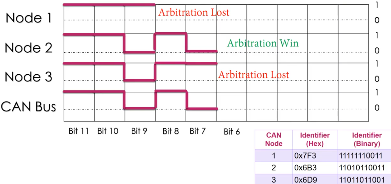
Illustrating the CAN Bus arbitrage mechanism based on the Identifier field
Thanks to this non-destructive arbitration mechanism, CAN Bus ensures that high-priority messages are always transmitted first without data retransmission, while maintaining the reliability and determinism of the system. This is why CAN Bus is widely used in real-time systems such as automotive control networks and industrial automation, where ensuring the order and latency of communication is crucial.
6. Error detection & Bus fault handing
Bit Error
bit error by transmitted
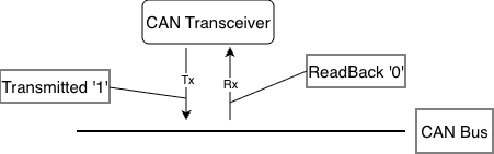
In the CAN protocol, every time a node transmits a bit onto the bus, it simultaneously “reads back” the bus’s state at that moment. In principle, if the transmitted value (TX) differs from the received value (RX), a Bit Error is detected. In the diagram above, the node is sending bit 1 but reading bit 0, which triggers a bit error. Bit errors can occur due to several reasons:
- Arbitration Process: This is the normal scenario; if two nodes transmit simultaneously, the node transmitting bit 0 (higher priority) will prevail over the node transmitting bit 1. When the node transmitting bit 1 sees a 0 on the bus, it understands it has “lost” the priority claim and stops transmitting to yield the right of way.
- Physical Fault: If this occurs in the data field or areas not eligible for adjudication, it could be due to: the CAN line is short-circuited to ground or power, excessive electromagnetic interference (EMI) causes voltage levels to fluctuate across the bus, the transceiver is broken.
When this error is detected (except during the arbitration phase), the node detecting the error will immediately send an Error Flag to notify all other nodes on the network that the current data is no longer trustworthy and needs to be retransmitted.
Stuff Error (Stuffing Error)
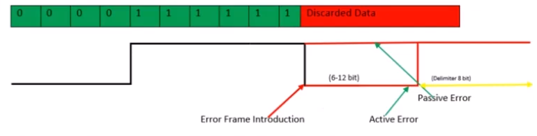
stuff error by receiver
To ensure that receivers can maintain synchronization with transmitters, the CAN protocol uses Bit Stuffing: This rule states that after every 5 consecutive bits with the same logic level (all 0 or all 1), the transmitter automatically inserts a reverse-biased bit to create “edges” (voltage level transitions) so that other nodes can readjust their internal clocks, avoiding clock misalignment when encountering a long, constant data stream.
This error occurs when a receiving node detects 6 consecutive bits with the same logic level on the bus (in areas where bit stuffing rules are applied, such as SOF to CRC). In your image, the bit sequence is 00000 (5 bits of 0), then instead of a stuff bit of 1, the bus displays consecutive 1 bits or other errors that violate the rule. When there are 6 bits of the same level (like the red “Discarded Data” segment), the receiving node identifies this as a Stuffing Error.
When a Stuffing Error is detected, the node will send an Error Frame to discard the current message: Error Frame Introduction: The moment the node detects the error and begins inserting error flags onto the bus.
- Active Error (6-12 bits): If the node is in the “Error Active” state, it will send 6 consecutive Dominant bits (level 0). Because other nodes will also see this 6-bit sequence as violating the Bit Stuffing rule, they will also send their own Error Flag, creating a sequence of 6 to 12 bits on the bus.
- Passive Error: If the node is in the “Error Passive” state (has encountered many errors before), it will send 6 Recessive bits (level 1). This does not interrupt the bus if other nodes are still operating normally. Delimiter (8 bits): After sending the error flag, the node will send an 8-bit Recessive (level 1) to signal the end of the error frame and prepare for retransmission.
As soon as an Error Frame appears, all previous data in the frame (Data Frame) is considered invalid and discarded by the receiving nodes. The transmitting node will have to retransmit the entire message from the beginning after the connection is stable again.
CRC Error
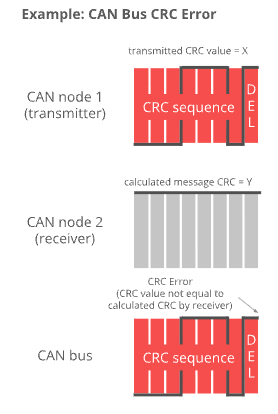
CAN Node 1 (Transmitter): The node that sends the message. It calculates a value based on the data content and sends it as a CRC Sequence (the transmitted value is X). CAN Node 2 (Receiver): The node that receives the message. Upon receiving the data, it performs a similar mathematical calculation on the received bits to produce the result Y (Calculated message CRC = Y). CAN Bus: The physical transmission medium where the CRC signal is transmitted.
CRC errors are detected at the receiver when the data is altered during transmission: If there is no interference, the value X (sent) should equal the value Y (recalculated). However, if one or more data bits are altered due to electromagnetic interference, the calculated value Y will differ from X. The image caption reads: “CRC Error (CRC value not equal to calculated CRC by receiver)”. This means that when X differs from Y, the receiving node identifies this as a CRC error. One key difference between CRC errors and other errors is the timing of their detection and processing:
- DEL (Delimiter) area: CRC errors are only checked after the entire CRC string has been received, specifically at the CRC Delimiter (CRC separator bit) location.
- Response: Immediately after the DEL bit, if the node detects an error, it will not send an ACK (Acknowledge) bit but instead will send an Error Frame to request the transmitting node to resend the data.
Acknowledgment Error (ACK Error)
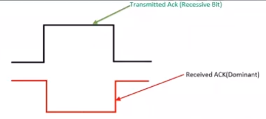
Unlike other communication protocols, in a CAN network, the receiver is responsible for confirming receipt of the data in the correct format. The transmitter sends a Recessive bit (level 1) at the ACK slot. Then, at the receiver, all nodes that receive the correct message (passing the CRC check) simultaneously pull their bus down to the Dominant level (level 0) at that moment to confirm receipt.
The diagram illustrates the contrast between the transmitted and received signals on the bus:
- Transmitted Ack (Recessive Bit): This is the signal from the transmitting node. It lets the bus go loose (level 1) and “listens” to see if any node acknowledges the connection.
- Received ACK (Dominant): This is the actual state on the CAN Bus. When at least one other node receives the data, it overwrites the bus with a 0.
- Normal result: The transmitting node reads back and sees level 0 (Dominant) even though I sent level 1 → Communication successful.
An ACK Error is acknowledged by the transmitting node when the transmitting node sends a Recessive (1) bit in the ACK slot but upon rereading the bus it is still at the Recessive (1) level, which means that no node on the network acknowledges receipt of that message.
Form Error
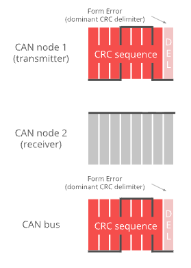
An error occurs when the structural components within a CAN data frame are misaligned at the logical level. In the CAN protocol, there are certain positions that must be Recessive bits (level 1) to mark the separation of message parts. A Form Error occurs when a receiving node detects a Dominant bit (level 0) at one of these fixed positions.
In your image, the specific error is indicated as:
Dominant CRC Delimiter: By standard, the DEL (Delimiter) bit immediately following the CRC sequence should always be a 1 (Recessive).
Phenomena: Both CAN node 1 (transmitter) and the CAN bus are displaying a 0 (Dominant) bit at this DEL position. Therefore, the system identifies this as a formatting error.
In addition to the CRC Delimiter position shown in the image, formatting errors can also occur at:
- ACK Delimiter: The delimiter bit after the acknowledgment slot (ACK Slot).
- End of Frame (EOF): A 7-bit Recessive sequence that ends a frame.
Similar to other errors, when a node detects a Form Error: It will transmit an Error Frame starting from the next bit.
The message being transmitted will be discarded: The transmitting node will increment the error counter and prepare to retransmit the message.
Bus Fault Handling
When an error is detected on the CAN bus, the system reacts immediately to protect data integrity and maintain network stability. CAN supports automatic error detection and a hierarchical fault-handling mechanism, enabling nodes to quickly detect anomalies and prevent faulty frames from propagating on the bus.
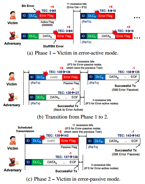
As illustrated in the figure, when a bit error or stuff error occurs, a node in the error-active state transmits an Active Error Flag, which interrupts the current frame and forces a retransmission. At the same time, the node’s Transmit Error Counter (TEC) is incremented, reflecting the severity of the error.
If the accumulated error count exceeds the predefined threshold, the node transitions to the error-passive state. In this state, the node transmits only a Passive Error Flag (recessive bits), reducing its impact on the bus while still allowing it to participate in communication. If subsequent transmissions are successful, the TEC gradually decreases, enabling the node to recover and return to the error-active state.
This mechanism demonstrates that CAN not only detects transmission errors but also automatically isolates and recovers faulty nodes, ensuring that correctly operating nodes can maintain stable communication. As a result, CAN achieves high reliability and is particularly suitable for safety-critical and real-time systems.
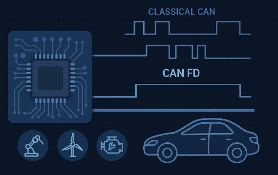
7. CAN FD Overview
CAN is short for ‘Controller Area Network’, and CAN FD is short for CAN with Flexible Data rate. Controller area network is an electronic communication bus defined by the ISO 11898 standards. In 2015 these standards were updated to include CAN FD as an addition to the previous revision, and the new reference number ISO 11898-1:2015(E) was assigned. The standard is written to make the information unambiguous, which unfortunately makes it hard to read because there are no extended descriptions or examples. The information in this tutorial is less formal, and designed to be easier to understand.
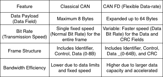
Collectively, this system is referred to as a CAN network, with Classical CAN and CAN FD as different Frame Formats supported by the standard.
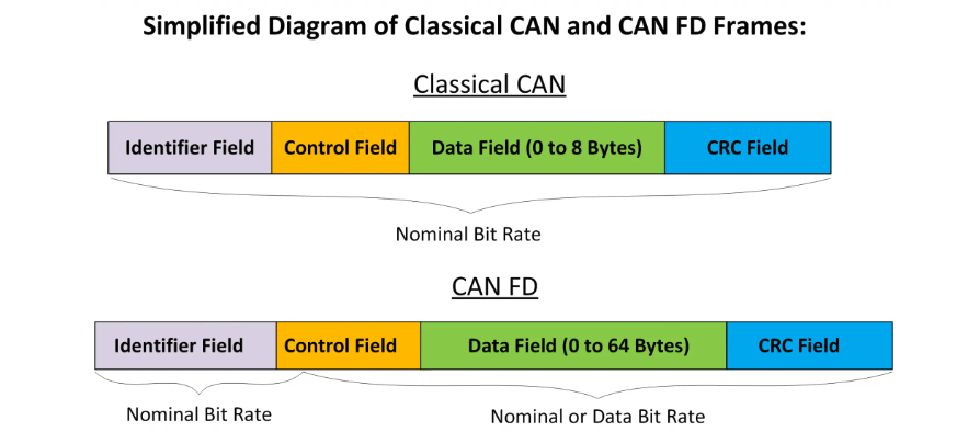
This diagram provides a visual comparison between two data transmission framework standards in control networks: Classical CAN and CAN FD. Below is a detailed description of the components:
8. Higher layer protocols on CAN
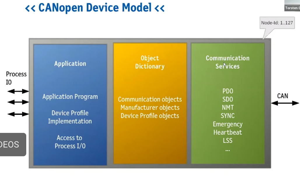
figure 1: data processing
The CANOpen device model is a standardized architecture that enables embedded devices to communicate uniformly within an industrial network. This architecture comprises three core components:
- The Application Layer: This is where application programs run and device profiles are executed to process data directly from physical input/output ports (Process I/O).
- The Object Dictionary: This acts as the central data management hub, storing communication objects, manufacturer objects, and device specifications.
Communication Services: This area is responsible for encapsulating and transmitting data over the CAN network using specific protocols such as PDO for real-time data transmission, SDO for configuration, and network management services like NMT, Heartbeat, and SYNC.
The entire model allows for the management of up to 127 nodes (Node-IDs) on the same network, creating high flexibility and compatibility between devices from various manufacturers.
In complex network control systems, the combination of device model and identification structure plays a crucial role in the stable operation of the entire system. Specifically, the CANopen device model provides a logical framework comprising the Application layer, Object Dictionary, and Communication Services to standardize how a device processes data. However, for these devices to accurately “identify” each other on the network without conflicts, the system needs an electronic “identity card” such as the NAME Field identification structure (according to the J1939/ISOBUS standard).
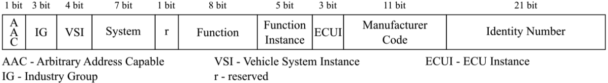
figure 2: identity verfication
Through this 64-bit string, information from the application layer such as device function, manufacturer code, and unique identifier number is tightly encapsulated. This connection allows communication services in the CANopen model to use detailed identifiers to perform automatic address claiming, making it easy for devices to integrate and communicate in real time as soon as they connect to the system.
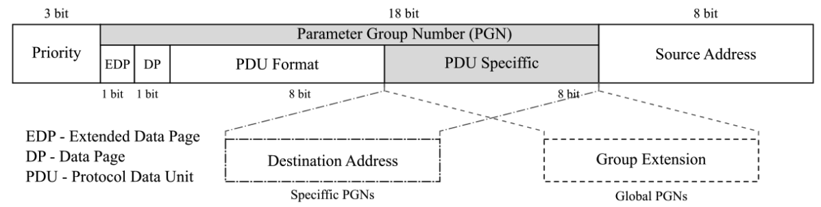
figure 3: the information to its correct destination
The CAN network communication system is a close coordination between device architecture, identity, and communication method:
First, the CANopen device model establishes the internal logic foundation, where data from the Application layer is managed in the Object Dictionary and ready to be transmitted through Communication Services. For a device to join the network, it needs a unique “identity” – a 64-bit NAME field. This structure contains information such as the Manufacturer Code and Function, allowing the device to automatically establish its identity and obtain a unique Source Address without conflict.
Finally, when the actual data is sent, the 29-bit Identity Framework directly coordinates the information on the transmission path. Here, the established source address is combined with the Priority and the number of Parameter Groups (PGNs) to precisely define the data type and destination. This linkage creates a complete cycle: from data processing at the device (Figure 1), identity verification (Figure 2), to shipping labeling to deliver the information to its correct destination (Figure 3).
9. Applications
9.1. CAN Bus (Classical CAN)
- CAN Bus (Classical CAN) – Automotive: CAN buses are widely used in automobiles to transmit data between ECUs such as the engine, ABS, airbags, transmission, and instrument cluster. For example, data from the Engine Control Unit can be transmitted to the Transmission, ABS, and Dashboard to control and monitor vehicle operation. The biggest benefit is reducing the number of wires in the vehicle and ensuring reliability through bus arbitration and error detection.
- CAN Bus – Industrial Automation: In industrial automation, CAN connects PLCs, sensors, and actuators. Typical applications include industrial robots, conveyors, and CNC machines. For managing more complex data, higher-layer protocols such as CANopen and DeviceNet are used, making device synchronization and management easier.
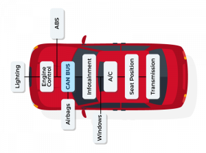
- CAN Bus – Medical Devices: Medical devices such as diagnostic imaging machines or patient monitors use CAN to transmit real-time data. CAN ensures accurate data with low latency, meeting stringent safety and reliability requirements.
- CAN Bus – Maritime & Aviation: In ships and UAVs, CAN is used to monitor and control engine, radar, and GPS systems. It provides stable communication, is resistant to electromagnetic interference, and is suitable for industrial or maritime environments.
- CAN Bus – Building Automation: CAN is also applied in smart building control, such as HVAC, lighting, and security systems. Thanks to its stable and robust communication capabilities, CAN helps reduce signal errors and increase reliability for automation systems.
9.2. CAN FD (Flexible Data rate)
- CAN FD – Automotive & High Data Applications: CAN FD (Flexible Data Rate) is an upgraded version of CAN, supporting larger frames (64 bytes) and higher transmission speeds. In modern automobiles, CAN FD is used to transmit data from cameras, radar, lidar, and infotainment systems. For example, ADAS (Advanced Driver Assistance Systems) systems use CAN FD to ensure real-time data, reduce the number of frames to be transmitted, and increase processing speed.
- CAN FD – Industrial Automation & High Throughput: In industry, CAN FD helps transmit multiple sensor and actuator data in a single frame, reducing latency and increasing system response speed. This is crucial for industrial robots, CNC machines, or devices requiring real-time data.
- CAN FD – ADAS & Autonomous Vehicles: CAN FD is the optimal choice for autonomous vehicles and advanced driver assistance systems where data from cameras, radar, and lidar needs to be transmitted continuously at high volumes. The large frame size and high speed of CAN FD ensure that data is processed promptly and accurately.
- CAN FD – Medical & Electric/Hybrid Vehicles: CAN FD is also used in MRI, CT, or multi-sensor monitoring devices where large amounts of image or data need to be transmitted quickly. In electric or hybrid vehicles, CAN FD helps manage the battery (Battery Management System) and sensors, transmitting battery status, temperature, and current data safely and at high speed.

10. Conclusion
CAN (Controller Area Network) is widely used because it provides reliable, fast, and cost-effective data communication. With its arbitration and error detection mechanisms, CAN ensures that critical data in embedded systems or vehicles is transmitted accurately and consistently, even in noisy environments.
One major advantage of CAN is its scalability and multi-node capability, allowing many devices to communicate on a single bus without excessive wiring, reducing cost and system complexity. Furthermore, with higher layer protocols such as CANopen, J1939, or DeviceNet, CAN not only transmits data but also supports device management, synchronization, and advanced fault handling, making it suitable for automotive, industrial, medical, and automation applications.
The advanced CAN FD provides larger data frames and higher data rates, meeting the demands of modern applications such as ADAS, electric/hybrid vehicles, industrial robots, and medical imaging systems. In summary, CAN is an ideal choice for any embedded system that requires high reliability, speed, and scalability.

BLE security – Security platform for modern IoT devices
1. Why is security necessary in BLE?
2. Security mode & Security Procedure in BLE
3. Authentication, encryption and delegation
4. Example – BLESA Attacks
5. Project on nRF52/nRF5340
6. Conclusion
1. Why is security necessary in BLE?
The widespread adoption of Bluetooth Low Energy (BLE) has played a key role in driving the development of IoT devices, wearables, and smart healthcare systems, bringing unprecedented levels of convenience and connectivity to modern life. With its advantages of low power consumption, reasonable deployment costs, and support across most popular platforms, BLE has quickly become the default choice for billions of connected devices globally. However, alongside this rapid growth are increasingly serious concerns about security and privacy.
Notably, most security risks associated with BLE do not stem from inherent weaknesses in the protocol itself, but rather primarily from how it is implemented in practice. The pressure to shorten time to market, coupled with the complexity of a Bluetooth specification spanning thousands of pages, sometimes forces developers and manufacturers to compromise between convenience, cost, and security. As a result, many critical security mechanisms are either inadequately configured or even omitted, creating subtle but potentially exploitable vulnerabilities.
In the context of Bluetooth Low Energy becoming an increasingly fundamental infrastructure in digital life—from personal devices and healthcare systems to industrial applications and smart infrastructures—understanding, implementing, and comprehensively evaluating BLE security mechanisms is no longer an option, but a necessity. Only when security is properly addressed from the design stage can BLE fully fulfill its role as a secure, reliable, and sustainable connectivity technology for the modern IoT ecosystem.
2. Security mode & Security Procedure in BLE
BLE security is built on two core concepts:
- Security Mode: defines the overall security strategy, i.e., the level of protection a connection or data requires.
- Security Procedure: the specific technical mechanisms used to implement that strategy.
In other words, the security mode determines “how much protection is needed,” while the security procedure answers “how to protect it.”
Security Mode 1 focuses on securing BLE connections through pairing and encryption. This mode includes four levels of security:
- Level 1: No authentication, no encryption – convenient but not secure.
- Level 2: Unauthenticated pairing with encryption (Just Works) – common but not MITM-protected.
- Level 3: Authentically authenticated pairing with encryption – MITM-protected through password entry or OOB.
- Level 4: LE Secure Connections – uses ECDH and a 128-bit key, the highest level of security.

Imagine an attacker being able to secretly modify the on/off switch of a communication device. This represents a potential Man-in-the-Middle (MITM) attack. Authentication helps protect against MITM by ensuring that each participating party can verify the other party’s identity cryptographically. In the BLE world, when you connect your smartphone to an IoT device for the first time, you might encounter a “pairing” pop-up window. Once the two devices are paired, they permanently save the settings and become “linked,” eliminating the need to re-pair each time they attempt to connect.

Passive eavesdropping and Man-in-the-Middle attacks are two of the most common types of cyberattacks involving hacking BLE modules. BLE networks can be attacked through passive eavesdropping, allowing an outside device to intercept data exchanged between devices. For example, an attacker could eavesdrop on data provided by industrial peripheral sensors to a central controller to discover new security vulnerabilities in the system. BLE modules using BLE Secure connections are, by default, protected against passive eavesdropping.
In MITM attacks, an alien device simultaneously assumes both central and peripheral roles, tricking other devices on the network into connecting to it. This can become a problem in large manufacturing complexes because the alien device can inject forged data into the data stream and disrupt the entire production chain. BLE Secure connections offer security against passive eavesdropping, but man-in-the-middle attacks can only be prevented with the right pairing techniques.
The level of security achieved largely depends on the device’s I/O capabilities and the trade-off between user experience and system security. Beyond connection security, BLE also supports data protection in specific contexts:
- Security Mode 2: uses connection-based data signing to ensure data integrity and authenticity, even without link encryption. This mechanism relies on CSRK and MAC keys to detect spoofing and replay attacks.
- Security Mode 3: applies to broadcast data, enabling broadcast data encryption using Broadcast_Code, particularly important for modern BLE broadcast applications (Bluetooth 5.4+).
3. Authentication, encryption and delegation
Bluetooth Low Energy security is built on three core mechanisms: authentication, encryption, and authorization. These three layers of protection work closely together to ensure that only legitimate devices can connect, that transmitted data is not exposed or modified, and that resource access is properly controlled.

Authentication in BLE verifies the identity of the connected devices, thereby preventing spoofing and MITM attacks. Authentication is performed during the pairing phase and may require user interaction through mechanisms such as password entry, number comparison, or Out-of-Band (OOB). Specifically, from BLE 4.2 onwards, the LE Secure Connections mechanism utilizes Elliptic Curve Diffie-Hellman (ECDH), enhancing MITM resistance and becoming the recommended authentication platform for modern BLE devices.

Encryption plays a crucial role in protecting data throughout wireless communication. After successful pairing, BLE devices generate secret keys and use the AES-CCM algorithm to encrypt the link, ensuring that data cannot be eavesdropped on or modified by third parties. Encryption helps protect not only application data but also the security keys exchanged during the connection, which is especially important for IoT and medical devices transmitting sensitive data.
Authorization is the next layer of protection after authentication and encryption, focusing on controlling resource access. In BLE, authorization is typically implemented at the GATT layer, where each service or characteristic may require a different level of security, such as only allowing read or write access when the connection is encrypted or authenticated. This mechanism ensures that even if a device has successfully connected, it can only access the resources it has been authorized to access.
The effective combination of authentication, encryption, and authorization determines the true security level of a BLE system. In practice, many security incidents stem not from a lack of these mechanisms, but from misconfiguration or inadequate use, highlighting the importance of thoroughly understanding and correctly implementing BLE security principles from the design stage.
4. Example – BLESA Attacks
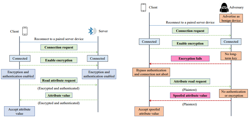
A prime example demonstrating the serious weaknesses of Bluetooth Low Energy, even with standard encryption mechanisms, is the BLESA (Bluetooth Low Energy Spoofing Attack) vulnerability, disclosed at the USENIX WOOT 2020 conference. According to the authors from Purdue University and EPFL, BLESA exploits the BLE reconnection mechanism – a feature designed to reduce latency and save energy for previously paired devices. In this scenario, the BLE standard does not require re-authentication of device identity during reconnection, allowing an attacker to impersonate a legitimate peripheral device and send forged data to the central device.
It is noteworthy that BLESA does not require encryption, does not require retrieval of the secret key, and does not rely on hardware errors. Instead, the attack exploits ambiguities in the BLE specification, allowing BLE stacks to implement reconnection mechanisms in various ways, some of which are insecure. Research indicates that BLESA can be successfully implemented on popular BLE implementations, including Linux BlueZ, as well as BLE stacks on Android and iOS, where the research team discovered logic flaws that allow the central device to accept connections from spoofed devices. These findings have been officially confirmed by Google and Apple, demonstrating the actual impact of the vulnerability.
transmission mechanism
According to the article, BLESA is particularly dangerous in common IoT scenarios such as wearables, medical sensors, and smart devices, where reconnection occurs frequently and completely automatically. Given that BLE is being used on billions of devices globally (estimated to reach over 5 billion BLE devices by 2023), BLESA demonstrates that secure initial pairing is insufficient. Without additional measures such as GATT access control, application-layer authentication, or reconnection limitations, a BLE device can still be compromised without the user’s knowledge.
The BLESA case highlights a crucial fact: BLE security depends not only on the encryption algorithm but also heavily on how the standard is implemented and configured in practice. This clearly demonstrates that serious vulnerabilities in BLE can stem from protocol design and connection logic, rather than from cryptographic algorithms, and further underscores the need for comprehensive BLE security assessments, especially in large-scale IoT ecosystems.
5. Project on nRF52 / nRF5340
Pairing & Bonding (Zephyr / nRF SDK)
- Turn on LE Secure Connections
- Require MITM protection
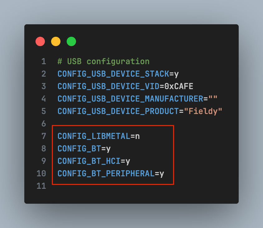
Protect GATT characteristic
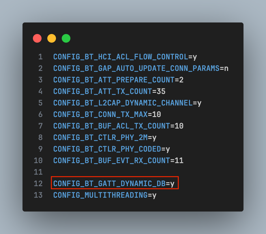
Bluetooth Security Manager Protocol
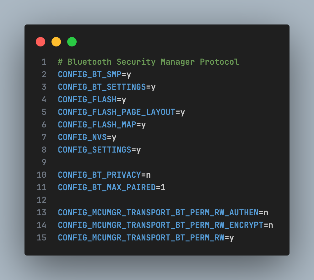
On nRF5340, CPUAPP handles the entire BLE security stack, allowing the combination of BLE + Secure DFU + TrustZone to build a multi-layered security system.
6. Conclusion
Only when properly implemented is Bluetooth Low Energy truly a secure wireless communication standard. Throughout the entire BLE connection lifecycle, the pairing phase remains the most sensitive point in terms of security, but it can be effectively protected if the correct pairing model and authentication mechanism are applied. Common threats such as man-in-the-middle attacks or passive eavesdropping mainly stem from weak security configurations, rather than from the BLE protocol itself.
In the development of IoT applications, the choice of hardware and software platforms plays a crucial role in the system’s security. SoCs like the nRF52 and nRF5340 provide all the necessary hardware security features for modern BLE, including LE Secure Connections, accelerated AES encryption, ECDH support, secure memory, and secure boot. When combined with properly deployed BLE stacks and tight coupling processes, these platforms enable the construction of energy-efficient and highly secure IoT systems in fields such as wearables, healthcare, industry, and smart homes.
For businesses considering deploying an IoT ecosystem, understanding and correctly applying security principles from the foundational level is essential. A secure IoT architecture must be built on reliable hardware and correctly configured protocols from the outset. In fact, it is common design and implementation vulnerabilities – not complex encryption algorithms – that cause the majority of serious security incidents and commercial losses.
How to build an image for STM32MP135
1. Yocto Project in STM32MP135
2. Environment setup
3. Add a new custom machine to Yocto
4. Add STMicroelectronics Layers to Yocto
1. Yocto Project in STM32MP135
In modern embedded Linux systems, the ability to tailor the operating system to specific hardware platforms is essential for optimizing performance, resource usage, and system reliability. The Yocto Project provides a powerful and flexible framework for building custom embedded Linux distributions that are reproducible, scalable, and maintainable.
This article describes the process of building a minimal embedded Linux system for the STM32MP135 processor on a custom System-on-Module (SOM). The workflow covers environment setup, Yocto Project configuration, custom machine integration, and image generation, enabling a reliable Linux platform tailored to the target hardware.
2. Environment setup
The system was developed on Ubuntu 22.04 LTS, the version recommended by Yocto and STMicroelectronics.
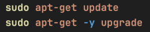
Before starting, you need to update your system to avoid library conflicts:
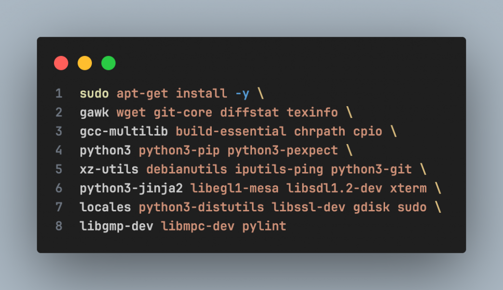
Yocto requires several tools for cross-toolchain, kernel, and rootfs builds. Important packages include:
- Compiler & build tools
- Python 3 and related modules
- Filesystem and image handling utilities
Installing all these packages ensures a stable build process, especially for initial builds. Packages required by OpenEmbedded/Yocto:
STMicroelectronics recommends using the en_US.UTF-8 locale to avoid errors during the build process:
![]()
3. Add a new custom machine to Yocto
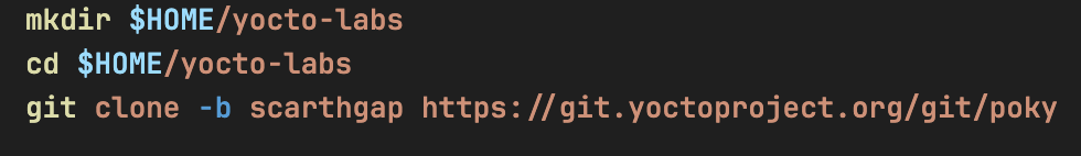
1. Download Yocto
Go to the address: $HOME/yocto-labs/
Download the scarthgap version of Poky:
2. Download STMicroelectronics Layers
Go to the yocto-labs directory, download meta-openembedded and meta-st-stm32mp layers:

3. Add new custom machine
Download the patch file to $HOME/yocto-labs/ and apply it
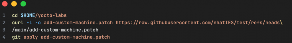
The patch adds a new custom machine (stm32mp1-ies) to the Yocto project. The patch performs the following tasks:
- Adds a new custom machine configuration to the meta-st-stm32mp layer
- Introduces a custom device tree for the new machine in the appropriate recipes, including:
– Trusted Firmware-A – U-Boot
– Linux kernel
– OP-TEE
4. Activate the build environment
Export all needed variables and set up the build directory:

4. Add STMicroelectronics Layers to Yocto
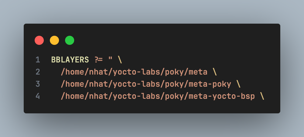
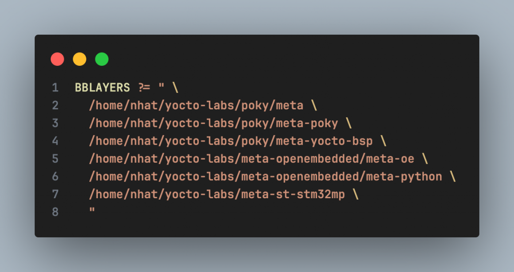
Added new layers to Yocto: In the build/conf/ directory, edit the bblayers.conf file. Initially, the file contains the following layers:
Add the following three layers to enable OpenEmbedded and STM32MP support:
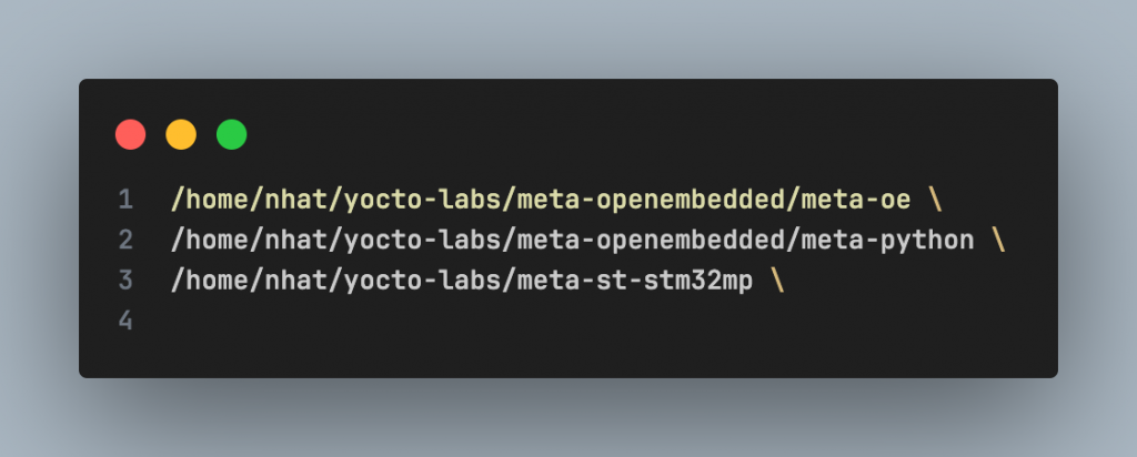
After the update, the bblayers.conf file should look like this:
1. Choose a target machine
You must specify which machine is your target (currently we use stm32mp1-ies). Go to $HOME/yocto-labs/build/conf/local.conf and set
![]()
2. Build the image
Now that you’re ready to start the compilation, go to the $HOME/yocto-labs/build/ and run:
![]()
Note: The first build process may take several hours, depending on the number of CPUs, available RAM, and Internet connection speed
3. Create the final image for SD Card
Once the build finished, you will find the output images under $HOME/yocto-labs/build/tmp/deploy/images/ stm32mp1-ies/
Execute the following command to create the final image for the SD card:
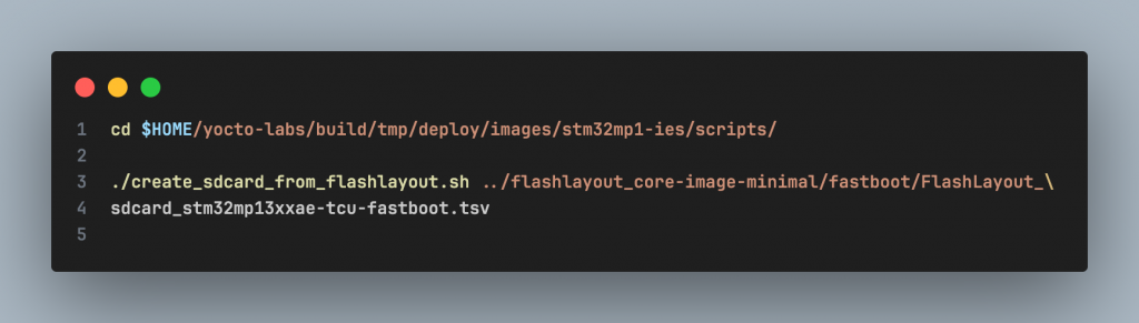
It will create the file FlashLayout_sdcard_stm32mp13xxae-tcu-fastboot.raw.
4. Flashing the image into the SD Card
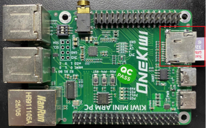
Insert the SD card into the PC via an SD card reader

Using Balena Etcher:

Insert the SD card into the board, then power on the board.
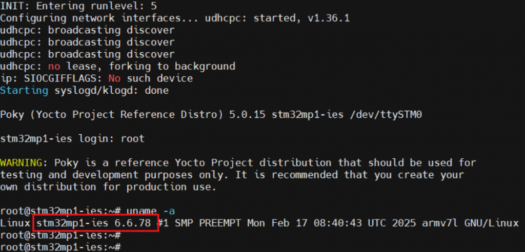
You should see the Linux boot log on the serial terminal.
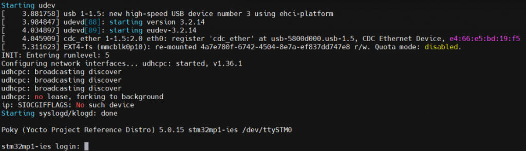
Wait until the login prompt, then enter root as user. Congratulations! The board has successfully booted.
You can verify the Linux kernel version by running

Since we are using the Scarthgap Yocto release, Linux kernel 6.6 is the expected version.
Edge AI for Predictive Maintenance: Unsupervised Vibration Anomaly Detection on MAX78000
1. AI Capability of ThingIQ
2. Data Acquisition and Signal Preprocessing
2.1. Vibration Sensor Overview
2.2. Signal sampling
2.3. FFT – Based Feature Extraction
3. AI Model Architecture
3.1. Model Tensor Description
3.2. Training
4. Deployment on MAX78000
5. Conclusion
1. Al Capability of ThingIQ
In modern industrial IoT systems, sensor data—particularly vibration data—plays a critical role in assessing equipment health. However, traditional monitoring approaches based on fixed thresholds are often inadequate in complex operating environments, where load conditions, rotational speeds, and environmental factors continuously vary.
ThingIQ leverages Artificial Intelligence (AI) as a core intelligence layer within its IoT platform, enabling early anomaly detection and predictive maintenance directly at the edge device, with low latency and high energy efficiency. Building on this foundation, ThingIQ adopts an AI-first approach, in which machine learning models are embedded directly into the IoT data processing pipeline. Rather than merely collecting and visualizing sensor data, the platform focuses on analysis, learning, and inference from real-time sensor streams.
This approach is particularly well suited for large-scale industrial and IoT systems, where operational requirements include:
- Early anomaly detection;
- Low-latency response;
- Reduced reliance on cloud-based inference;
- Optimized energy consumption.
To enable reliable and data-driven intelligence, the effectiveness of AI models fundamentally depends on the quality and structure of input data. In industrial environments, raw sensor signals are often noisy, non-stationary, and highly dependent on operating conditions. Therefore, a robust data acquisition and signal preprocessing pipeline is a critical prerequisite for meaningful learning and inference. The following section describes how vibration signals are acquired and transformed through signal preprocessing techniques to extract informative representations for subsequent AI-based analysis.
2. Data Acquisition and Signal Preprocessing
One of ThingIQ’s key AI capabilities is vibration-based anomaly detection, built upon a signal processing and deep learning pipeline designed for industrial IoT environments. Vibration data is acquired in real time from accelerometer sensors and transformed into the frequency domain using the Fast Fourier Transform (FFT). Frequency-domain analysis highlights characteristic vibration patterns associated with normal operating conditions of industrial equipment.
After FFT processing and normalization, the data is fed into a Convolutional Neural Network (CNN) Autoencoder, where the model learns to reconstruct normal vibration patterns. The reconstruction error is then used as a quantitative metric to detect operational anomalies.
This approach enables the system to:
- Detect subtle deviations before physical thresholds are exceeded
- Adapt to changing operating conditions
- Reduce false alarms compared to traditional rule-based methods
2.1. Vibration Sensor Overview
The vibration data is collected using a 3-axis MEMS accelerometer mounted directly on the mechanical structure under monitoring
The sensor measures linear acceleration along three orthogonal axes:
- X-axis: Typically aligned with the horizontal direction
- Y-axis: Typically aligned with the vertical direction
- Z-axis: Typically aligned with the axial or radial direction of the rotating shaft
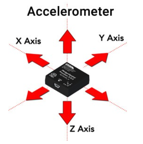
Figure 1: Accelerometers Measure Acceleration in 3 Axe
2.2. Signal sampling
Each axis of the accelerometer produces an analog vibration signal, which is digitized using the MAX78000 ADC.
Typical sampling parameters:
- Sampling frequency (Fs): 20 kHz – 50 kHz
- ADC resolution: 12 bits
- Anti-aliasing filter: Analog low-pass filter applied before the ADC input
The sampling frequency is selected according to the Nyquist rule to ensure that all fault-related vibration frequencies are captured without aliasing.
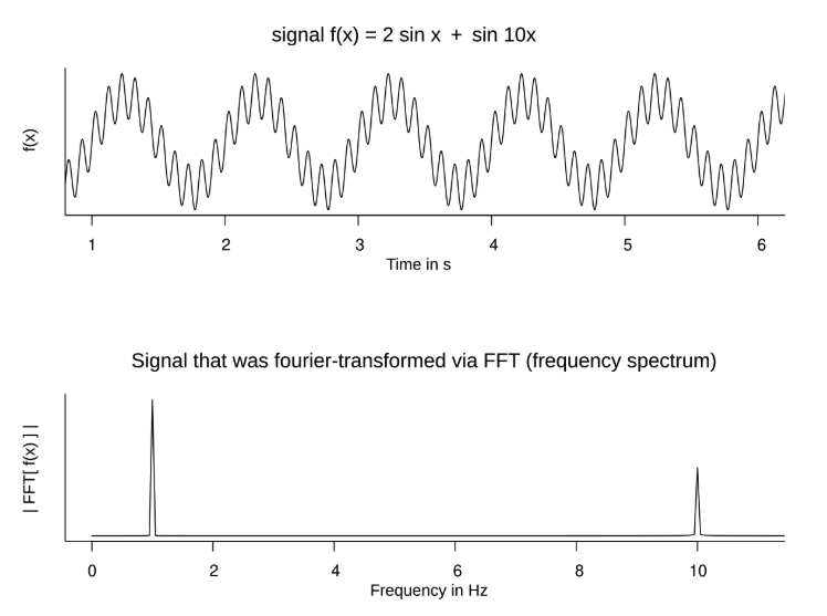
2.3. FFT – Based Feature Extraction
After sampling, the vibration signals from each axis (X, Y, and Z) are transformed from the time domain into the frequency domain using the FFT. Each axis is processed independently.
The FFT converts raw vibration signals into frequency bins, where mechanical faults typically appear as distinct spectral components. Only the magnitude of the FFT is used, as phase information is not required for vibration-based fault detection.
This frequency-domain representation provides compact and informative features that are well suited for predictive maintenance and subsequent AI-based analysis.
3. AI Model Architecture
3.1. Model Tensor Description
Technical Description of Model Input and Output:
- Model Input Shape: [256, 3] (representing [Signal_Length, N_Channels]).
- Input Details: The input consists of 3 axes (X, Y, and Z), where each axis contains 256 frequency bins (FFT data points).
- Model Output Shape: [768, 1].
- Output Details: The final layer is a Linear layer that produces a flattened output of 768 features (calculated as 256 3).
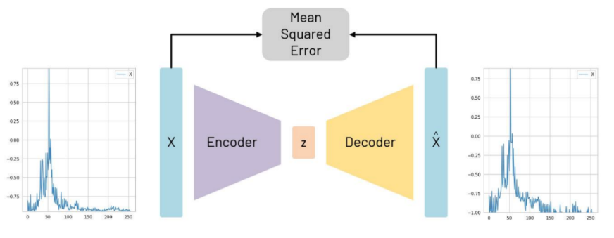
Figure 2: Autoencoder structure, with reconstruction of an example X axis FFT shown
3.2. Training
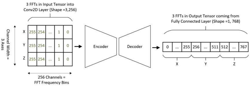
Figure 3: Input and output tensor shapes and expected location of data
In general, a model is first created on a host PC using conventional toolsets like PyTorch and TensorFlow. This model requires training data that must be saved by the targeted device and transferred to the PC. One subsection of the input becomes the training set and is specifically used for training the model. A further subsection becomes a validation set, which is used to observe how the loss function (a measure of the performance of the network) changes during training.
Depending on the type of model used, different types and amounts of data may be required. If you are looking to characterize specific motor faults, the model you are training will require labeled data outlining the vibrations present when the different faults are present in addition to healthy vibration data where no fault is present.
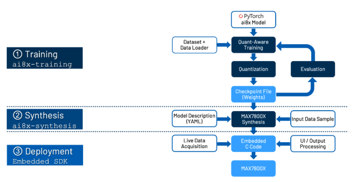
As a result of this process, three files are generated:
- cnn.h and cnn.c
These two files contain the CNN configuration, register writes, and helper functions required to initialize and run the model on the MAX78000 CNN accelerator. - weights.h
This file contains the trained and quantized neural network weights.
4. Deployment on MAX78000
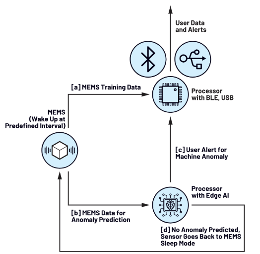
Figure 5: mode of operation
Once the new firmware is deployed, the AI microcontroller operates as a finite state machine, accepting and reacting to commands from the BLE controller over SPI.
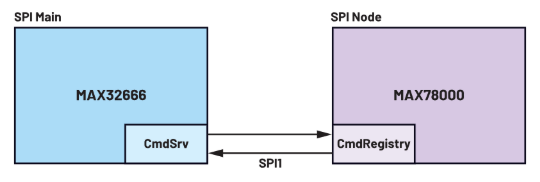
When an inference is requested, the AI microcontroller wakes and requests data from the accelerometer. Importantly, it then performs the same preprocessing steps to the time series data as used in the training. Finally, the output of this preprocessing is fed to the deployed neural network, which can report a classification.
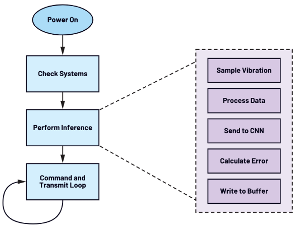
Figure 6: AI inference state machine
5. Conclusion
By integrating advanced signal processing techniques with deep learning, ThingIQ provides a robust and scalable approach to vibration-based anomaly detection for industrial IoT systems. The combination of FFT-based feature extraction, CNN autoencoder modeling, Quantization Aware Training, and edge AI deployment enables early detection of abnormal behavior with low latency and high energy efficiency.
This architecture allows enterprises to move beyond reactive, threshold-based monitoring toward proactive, data-driven operations, establishing a solid foundation for predictive maintenance and intelligent asset management in large-scale IoT environments.

ThingIQ – A comprehensive IoT platform
1. What is ThingIQ?
2. IoT platform ThingIQ
3. Integrate AI with ThingIQ
4. Conclusion
1. What is about ThingIQ?
“UPGRADE YOUR IOT FUTURE”

Market tendency – Insight – Action
Over the past decade, the Internet of Things (IoT) has undergone rapid development, from simple monitoring systems to infrastructures connecting millions of devices. However, as IoT matures, the core challenge is no longer data collection, but the ability to transform that data into tangible operational value.
The explosion of sensor data, real-time data, and complex data streams has rendered traditional management models ineffective. In this context, integrating artificial intelligence (AI) into IoT platforms is no longer a trend, but a necessary market requirement.
Faced with this reality, ThingIQ defines its vision: to build an IoT platform that not only connects devices but also supports businesses in making intelligent decisions based on data and AI. Instead of focusing on purely displaying data, ThingIQ’s vision is to bridge the gap between operational data and action, where analytical models and machine learning play a central role in anomaly detection, trend prediction, and system performance optimization. Therefore, the ThingIQ platform is conceived as an AI-integrated IoT solution right from the architectural design stage. Instead of building a connected system and then adding AI later, ThingIQ is developed with an AI-first philosophy, where IoT data is processed, analyzed, and continuously learned to generate actionable insights.

ThingIQ is geared towards large-scale IoT systems where stability, scalability, and integration with existing infrastructure are essential. Based on this vision, ThingIQ is built with a clear layered architecture, enabling real-time collection, processing, and analysis of IoT data, while integrating AI models to support intelligent operation.
2. IoT platform ThingIQ
As IoT systems expand from the experimental stage to real-world deployment, businesses quickly face systemic challenges. These pain points don’t stem from individual devices, but rather from management, operation, the environment, and integration capabilities across the entire IoT infrastructure.
ThingIQ is built to directly address these issues through three core solution groups:
- Intelligent Management & Operations;
- Environmental & Security Solutions;
- IoT Connectivity & API Integration.
For businesses operating hundreds to thousands of dispersed assets such as vehicle fleets, machinery, and industrial equipment, data often comes from multiple sources and protocols, lacking standardization and difficult to utilize effectively. Manual monitoring leads to slow response times, reactive maintenance, and uncontrollable costs. ThingIQ addresses this problem with its intelligent Management & Operations platform, enabling real-time fleet monitoring (GPS, speed, fuel level, engine status via OBD-II and LTE SIM) as well as continuous monitoring of industrial equipment. Data is standardized and processed on an IoT cloud platform, enabling businesses to remotely monitor, analyze operating behavior, support predictive maintenance, and improve asset utilization efficiency.
Devices Management interface ThingIQ
In environments such as smart buildings, factories, and cold storage facilities, a lack of real-time environmental monitoring can lead to significant risks to quality, safety, and energy waste. Temperature, humidity, and energy consumption data are often fragmented, making it difficult for businesses to meet increasingly stringent standards. ThingIQ provides a comprehensive building, energy, and environmental management solution that enables real-time data monitoring and analysis, operational automation, and threshold alerts. This allows businesses to ensure compliance, protect product quality, reduce risks, and move towards sustainable operations at optimal cost.

In recent years, air quality in Hanoi has consistently been poor, especially during transitional seasons and peak traffic times, with concentrations of fine particulate matter and air pollutants exceeding recommended levels. This situation not only affects public health but also directly impacts labor productivity and the quality of life. ThingIQ’s IoT-based air quality monitoring solution allows for continuous real-time tracking of pollution indicators, CO₂, humidity, and temperature, enabling businesses, urban areas, and management agencies to proactively assess risks, issue early warnings, and implement timely and effective environmental improvement measures.

Air quality in Hanoi at the beginning of 2026
One of the biggest challenges for enterprise IoT is the fragmentation of devices, protocols, and systems, which isolates data and makes integration with existing platforms like ERP, MES, or BI difficult. ThingIQ addresses this problem through its IoT API Gateway – a secure and scalable middleware that bridges devices, cloud platforms, and enterprise applications. The gateway supports protocol conversion, centralized device management, and real-time data exchange, enabling businesses to seamlessly integrate IoT ecosystems, maintain openness and scalability, and ensure long-term data security.

3. AI in ThingIQ
ThingIQ integrates AI as a foundational component in its IoT architecture, transforming multi-source sensor and operational data into exploitable knowledge. Machine learning models are deployed directly in the data processing pipeline, allowing the system to learn from the real-world operating behavior of devices and the environment, rather than relying on thresholds or static rules.
The AI in ThingIQ focuses on core analytical problems of enterprise IoT, including contextual anomaly detection, trend analysis, and device state prediction. Through learning from historical and real-time data, the platform supports predictive maintenance, reduces unplanned downtime, and optimizes asset lifecycles.
ThingIQ’s approach aims for AI that is controllable and explainable, ensuring compliance with operational requirements and data security. AI not only serves for display purposes, but also acts as a decision support layer, helping businesses shift from passive monitoring to proactive, data-driven operations.
For example, when comparing two systems, one with AI integration and one without, the advantages of AI applications become clear:
- For IoT systems without AI: Traditional systems are primarily based on data collection and fixed thresholds. Sensors send data (temperature, humidity, equipment status) to a central platform, where the data is displayed on a dashboard and triggers alerts when predefined thresholds are exceeded. This approach is suitable for basic monitoring but is limited in complex operating environments where operating conditions change constantly. The system only reacts after an incident has occurred, easily leading to false alarms and making it difficult to support optimal operation or proactive maintenance.
- Case 2: IoT systems with AI (ThingIQ) are integrated into the ThingIQ platform. IoT data is not only monitored but also analyzed contextually. Machine learning models study the normal operating behavior of equipment and the environment, thereby detecting anomalies early even before values exceed thresholds. AI allows for forecasting trends and equipment status, supporting predictive maintenance and operational optimization. Instead of reacting passively, businesses can proactively make decisions based on data and forecasts.
From there, we get a comparison table to better understand the AI features:

4. Conclusion
In the short term, ThingIQ focuses on developing and deploying comprehensive IoT solutions, helping businesses quickly solve real-world operational challenges, optimize asset, environmental, and system management, while ensuring flexible and stable deployment.
In the long term, ThingIQ aims to build an AI-integrated IoT platform as the core data infrastructure for businesses, where data is analyzed in depth to support intelligent decision-making, operational automation, and sustainable growth.
In terms of expertise and commitment, the ThingIQ team possesses comprehensive capabilities ranging from hardware design and development, IoT connectivity system deployment, to cloud integration and operation. By leveraging advanced connectivity protocols and in-depth data analysis, we deliver smarter, more efficient, and future-ready industrial solutions.
ThingIQ is committed to quality, innovation, and customer satisfaction at every stage, from design and implementation to system operation and scaling!
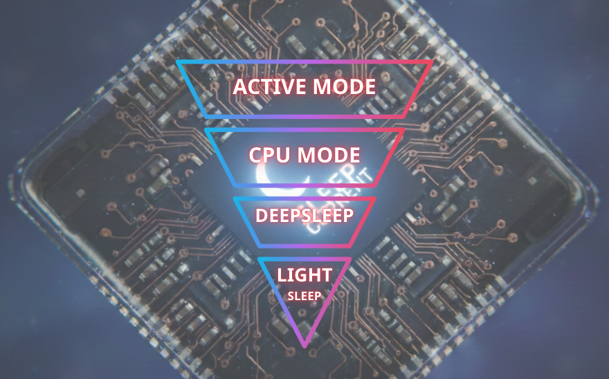
Sleep Current of XIAO nRF52840
1. Introduction
2. Sleep current in practice
2.1. Measuring tool
2.2. Understanding sleep currents correctly
3. Conclusion
1. Introduction
In IoT systems and battery-powered devices, microcontrollers spend most of their time in a dormant state, so sleep current – the current consumed when the system is “sleeping” – often has a much greater impact than the current consumed when operating. Especially with applications like BLE beacons, sensor nodes, or wearables, devices can sleep for over 99% of their operating time, meaning even a few microampere differences in sleep current can significantly alter battery life from a few months to several years. Nordic Semiconductor’s nRF52840 is known as a BLE SoC with very low power consumption, with sleep current values in the microampere range as stated in its datasheet. However, in practice, many projects have reported much higher current consumption than expected, even reaching hundreds of microampere or several milliampere values despite the firmware putting the system to sleep. The main reason is that CPU-level sleep is not synonymous with system-level sleep: clocks, peripherals, BLE radios, GPIOs, or external hardware components can still run in the background and continuously wake the SoC. Furthermore, datasheets often reflect ideal measurement conditions, while the actual system is a combination of firmware, BLE configuration, hardware, and measurement methods. This article aims to clarify the nature of sleep current on the nRF52840, highlight the differences between theory and actual measurements, and provide a systematic approach to analyzing, measuring, and optimizing current consumption down to the microampere level in practical applications.
2. Sleep current in practice
2.1. Measuring tools
Nordic Semiconductor’s Power Profiler Kit II (PPK2) is an affordable hardware and software tool that helps engineers flexibly measure power consumption for IoT devices, especially with the Nordic nRF chip, allowing simultaneous viewing of both average and high-current event data with a faster sampling rate (100ksps), integrated via the nRF Connect application on a PC for more efficient energy analysis and optimization.
The Power Profiler Kit II (PPK2) is a specialized power consumption measurement tool developed by Nordic Semiconductor, designed for energy analysis and optimization in low-power embedded systems. This device provides high-accuracy current measurement capabilities, particularly suitable for battery-powered IoT applications.
![]()
Key features of the PPK2 include:
- Flexible current measurement, supporting both average current and peak current modes, allowing for detailed analysis of system power consumption behavior.
- High sampling rate, up to 100 kSamples/s, approximately 10 times faster than the previous generation, enabling clear observation of very short power consumption events such as radio on/off, wake-up, or interrupt handling.
- The included software, integrated into the nRF Connect for Desktop Power Profiler application, allows for visual real-time display of measurement data and supports data export for further analysis.
- A 10-pin logic interface allows monitoring logic signals from the test device (DUT) synchronized with current consumption data, useful for linking firmware behavior to current spikes during energy optimization.
- The PPK2 has a wide range of applications, particularly effective in optimizing energy consumption for BLE, LTE-M, and NB-IoT devices, and is often used with development kits such as the nRF9160.
The basic operating principle of the PPK2 is quite simple: the device is connected to a computer via a Micro-USB cable and to the DUT using jumper wires to both power and measure current consumption. Users utilize the nRF Connect Power Profiler application on their PC to configure the measurement mode, observe the current graph over time, and thus detect periods of high or low energy consumption in the system’s operating cycle.
The target users of the PPK2 are primarily hardware and software engineers developing battery-powered IoT products, as well as those who need to analyze and optimize battery life for low-power applications where every microampere counts.
2.2. Understanding sleep currents correctly
To clarify the information related to Sleep Current, we measured the nRF52840 using the Nordic Power Profiler Kit II (PPK2) at a sampling rate of 100 kS/s over a period of 10 seconds, yielding the following results:
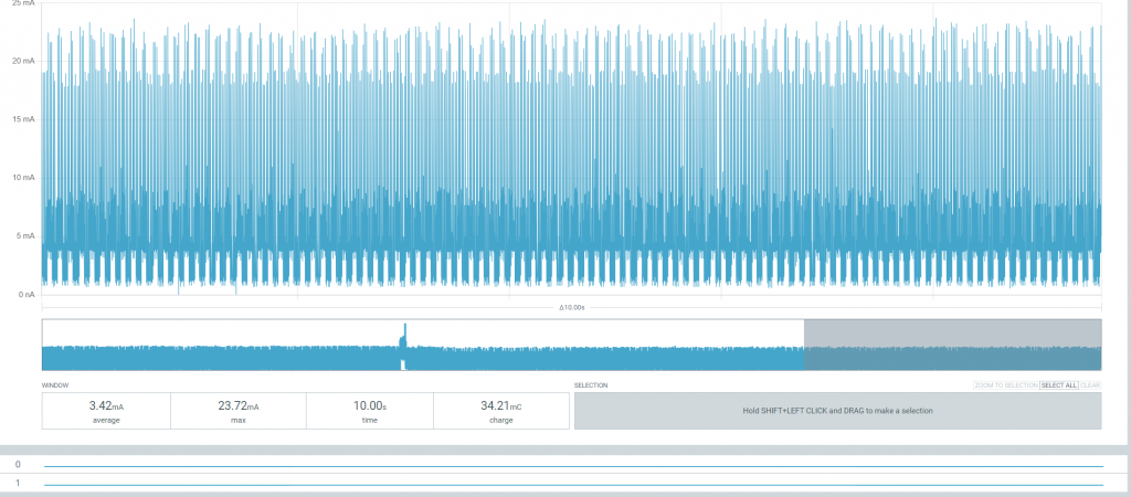
Overall view: “The device is not really sleeping”
Observation shows that the current fluctuates continuously from ~0 mA to ~20+ mA, with no “flat” segment at the µA level; the pulse density is high, uniform, and repeats periodically. This is not true sleep, but rather a CPU sleep mode while the radio/clock/background tasks are still running. This indicates that the device is being woken up periodically; even though the firmware has invoked sleep, the current consumption still varies significantly with mA‑level spikes. This proves that ‘sleep’ at the CPU level does not equate to low power at the system level.
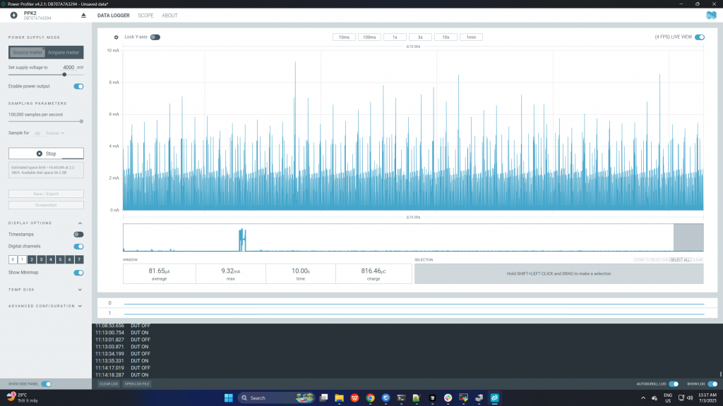
For this case, the “thought it was sleeping” case: the average is low but the underlying behavior is still wrong. It’s easy to see that the measured parameters include: average current: ~81.65 µA, peak: ~9.32 mA, Measurement time: 10 s, charge: ~816 µC. Next, looking at the waveform, the baseline is quite low (µA–tens of µA) but there are still mA-level spikes appearing continuously and there is no stable flat-line segment. The device has not really entered a proper System ON low-power mode; the BLE radio or timer is still active, and the sleep current does not reach the datasheet level. Although the average current is only about 80 µA, the waveform shows that the device is still generating periodic mA-level spikes. This is a common mistake: evaluating sleep current only based on the average value while ignoring the actual behavior of the system.
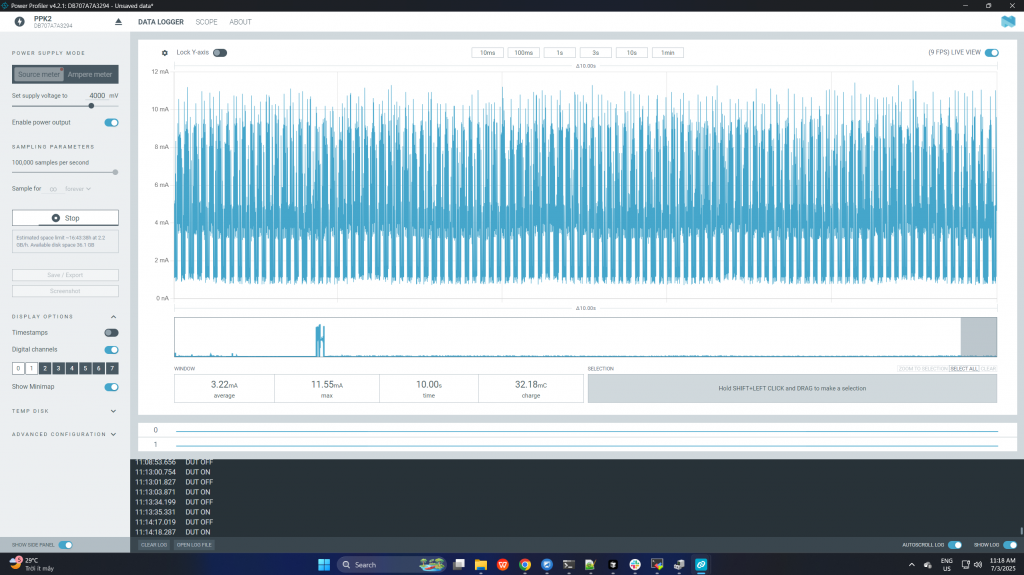
Finally, let’s look at this figure: the Active / BLE-heavy state (reference) with parameters: average: ~3.22 mA, peak: ~11.55 mA, charge: ~32.18 mC / 10 s. This corresponds to a state of dense BLE advertising or a short BLE connection interval, where the CPU + radio are operating frequently, showing the current consumption when the device is actively running. Notably, the waveform of the “non-optimized sleep” state (previous picture) has a shape very similar to this active state.
3. Conclusion
Sleep current is often treated as a single number quoted from a datasheet, but practical measurements on the nRF52840 show that it is a system-level characteristic, not merely a CPU state. Through real measurements using the Nordic Power Profiler Kit II (PPK2), this article demonstrates that a device can appear to be “sleeping” at the firmware level while still consuming significant energy due to periodic wake-ups, active clocks, BLE radio activity, or misconfigured peripherals.
The measurement results clearly show three distinct behaviors: a fully active BLE-heavy state with continuous milliampere-level current, a misleading “average-low-current” state where the baseline is low but frequent mA-level spikes persist, and a properly optimized sleep configuration where the system finally approaches the microampere-level currents stated in the datasheet. This highlights a common pitfall in low-power design: relying solely on average current values without examining the actual current waveform can lead to incorrect conclusions about battery life.
Using a high-resolution measurement tool such as PPK2 is therefore essential. Its high sampling rate makes short current spikes visible, enabling engineers to correlate power consumption with firmware behavior and identify hidden wake-up sources. Only by analyzing both the shape of the current waveform and the statistical values (average, peak, and charge) can true low-power operation be verified.
In conclusion, achieving datasheet-level sleep current on the nRF52840 requires a holistic approach that combines correct firmware sleep states, careful BLE configuration, proper clock and peripheral management, and clean hardware design. When these factors are addressed together—and validated with accurate measurement tools—microampere-level sleep current is not only theoretical but achievable in real-world IoT applications.
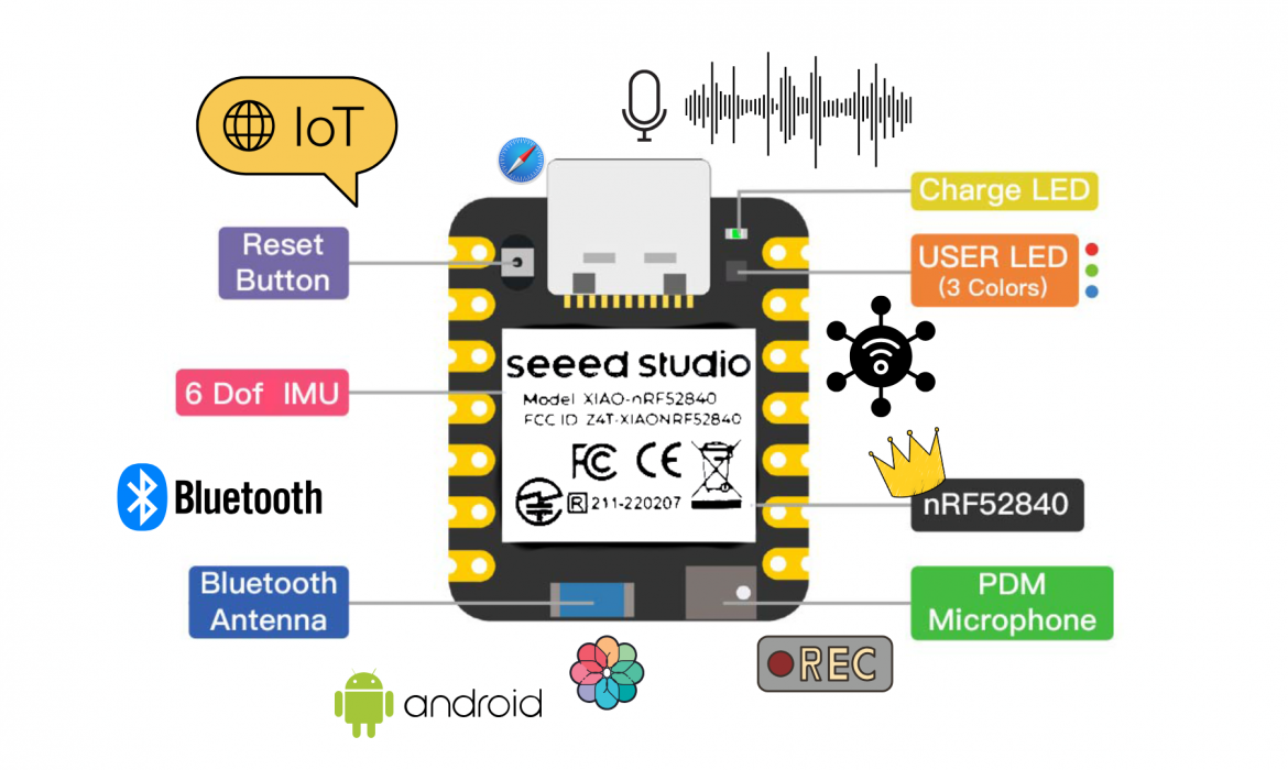
Microphone & Audio Processing Pipeline in nRF52840
1. Introduction
1.1. Introduce about nRF52840
1.2. Analog microphone vs PDM microphone
2. Mono and Stereo hardware
2.1. Mono mode
2.2. Stereo mode
3. Data processing stream
4. Conclusion
1. Introduction

1.1 Introduce about nRF52840
Seeed Studio XIAO nRF52840 is the first wireless board in the XIAO series, featuring the Nordic nRF52840 SoC with Bluetooth Low Energy 5.0 support. Its ultra-compact form factor, single-sided SMD design, and integrated Bluetooth antenna make it well-suited for mobile devices and rapid IoT prototyping.
The XIAO nRF52840 Sense variant integrates a digital PDM microphone and a 6-axis IMU, enabling real-time audio capture and motion sensing. These onboard sensors make it ideal for TinyML applications such as voice recognition, acoustic event detection, and gesture recognition. The upgraded XIAO nRF52840 Plus and Sense Plus versions further enhance usability by increasing the number of multifunctional pins to 20, adding I2S and SPI resources, exposing NFC pins, and optimizing the BAT pin placement for easier soldering and power integration. The board provides rich interfaces including UART, I2C, and SPI, with 11 digital (PWM) pins and 6 analog (ADC) pins, along with 2 MB of onboard flash memory. It supports multiple development environments such as Arduino, MicroPython, CircuitPython, and Zephyr SDK.
Typical Applications:
- Bluetooth Low Energy (BLE): low-power IoT devices, beacons, wearables, sensor data streaming
- Voice & Audio Processing: audio capture, voice recognition, keyword spotting
- Recorder: local audio recording or BLE audio transmission
- TinyML: gesture recognition, audio classification, edge AI
1.2. Analog microphone vs PDM microphone
In the nRF52840, both analog microphones and PDM (Pulse Density Modulation) microphones can be used. However, PDM microphones are generally preferred for high-quality digital audio applications such as audio-based machine learning. While analog microphones require an external ADC for signal digitization, PDM microphones output digital data directly. This allows tighter integration with the MCU, higher overall performance, improved noise immunity, and reduced GPIO usage—especially when using advanced PDM drivers provided by mbed OS or the Nordic SDK.
For analog microphones, to better understand their operating principle, we consider a typical circuit based on an electret microphone with a simple yet effective signal amplification structure. The electret microphone is powered through a bias resistor Rbias (typically in the range of 2.2 kΩ to 10 kΩ) connected from VDD to the signal pin. This biasing provides the correct operating conditions for the internal FET transistor inside the microphone.
The microphone produces an AC audio signal, which is separated from the DC component by a coupling capacitor C₁ before being fed into the op-amp input. At this stage, resistor R₁ sets the input impedance and, together with the op-amp, forms an amplification stage. Meanwhile, the VDD supply is stabilized using a bypass capacitor to reduce power-supply noise and prevent it from affecting the output signal.
With this configuration, the audio signal captured from the microphone is amplified in a stable manner, exhibits reduced noise, and achieves sufficient quality for further processing or digitization in subsequent stages. The overall circuit can be modeled as follows:
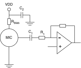
Diagram Analog microphone
For PDM microphones, the operation follows the principle of digital pulse density modulation. The PDM microphone is powered via the VDD pin and connected to ground at the GND pin. Once the acoustic signal is captured, it is directly converted into a PDM bitstream inside the microphone and transmitted to the host circuit through the Data pin. The microphone’s operation and data synchronization are controlled by a Clock signal provided by the host and applied to the Clock pin of the microphone. In addition, the SEL (Select) pin—typically connected to the host circuit—allows selection between the Left or Right channel when multiple microphones share the same PDM bus. If only a single microphone is used, this pin can be fixed to a defined logic level by pulling it up or down through an appropriate resistor. To ensure signal stability and minimize noise, a bypass capacitor is usually placed close to the microphone’s VDD pin to filter power-supply noise. With this configuration, the system achieves stable digital audio capture, where data is streamed directly into the processing block without requiring an intermediate analog amplification stage. The overall structure can be summarized by the following block diagram:
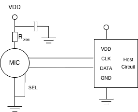
Diagram PDM microphone
The choice of using MEMS microphones with analog or digital output signals often depends on how the output signal will be used. Analog output signals are convenient if they are connected to an amplifier input for analog processing in the host system. Examples of common analog applications are simple loudspeakers or radio communication systems. MEMS microphones with analog outputs also tend to consume less power than microphones with digital outputs due to the absence of an ADC converter.
2. Mono and Stereo hardware
Based on the operating principle of PDM microphones, the audio signal is already digitized inside the microphone and streamed directly to the microcontroller via the PDM interface. This significantly simplifies the analog front-end and enables flexible microphone configurations. On the nRF52840 platform, the dedicated PDM hardware peripheral supports both mono and stereo microphone setups, making it suitable for a wide range of applications such as voice recognition, audio recording, and spatial audio processing. The following section describes in detail the hardware configurations for mono and stereo PDM microphones.
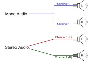
Mono mode vs Stereo mode
2.1. Mono mode
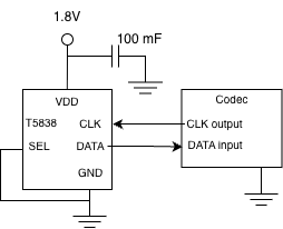
Connect Mono with Codec
Mono (Monophonic) is an audio effect where sound is captured and played from a single source. Because it comes from a single source, it can be difficult to distinguish the location of the sound in space.
Fieldy firmware supports mono mode via both software and hardware:
- For hardware: Fieldy uses only one PDM microphone; the SEL pin of the microphone is fixed because it only uses one channel, and the MCY only reads one DATA stream.
- The microphone connects directly to the nRF52840’s PDM peripheral; it does not use an ADC or an external audio codec for recording.
Configuration of samples rate suitable voice:
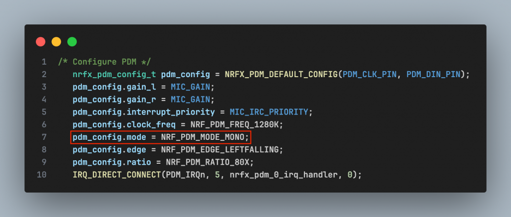
Configuration of PDM in Mono mode
In the driver microphone (mic.c):

mic.c settings
Calculate from here frequency for mono PCM is 16 KHz The suffer PCM 1 channel:
Besides, supporting mono mode in codec:
Opus encoder mono
No parameter for channel, PCM default is mono:
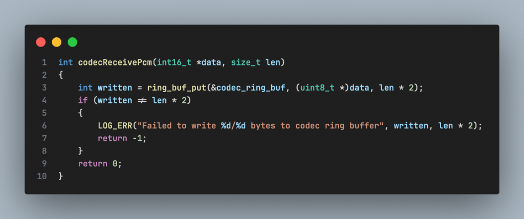
Codec API support only mono mode
Next, Fieldy firmware supporting in configuration the systems in this file config:
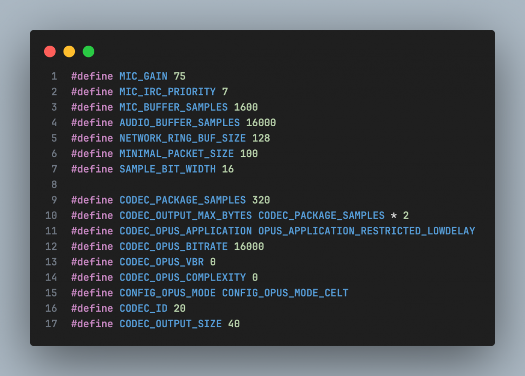
Configuration audio system
The audio system is configured for single-channel (mono) voice capture and encoding with a sampling frequency of 16 kHz. 16-bit PCM data is packed into 20 ms frames and compressed using the Opus codec in CELT mode, with a fixed bitrate of 16 kbps, to optimize low latency, low power consumption, and suitability for data transmission over BLE.
2.2. Stereo mode
Stereo sound is audio that is reproduced from two separate sound channels, played through a speaker system with a two-speaker configuration, or through headphones, allowing the listener to perceive the spatial position of sounds. Stereo sound is associated with spatial positioning through the variation of sound between the two component speakers, helping to distinguish left/right sound positions effectively.
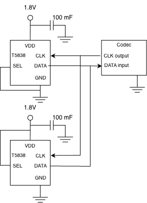
Stereo mode
The nRF52840 MCU supports stereo audio recording via the PDM peripheral. However, in 6 the current Fieldy hardware design, only one PDM microphone is used and it is configured in mono mode. To implement stereo mode, a second microphone needs to be added or a stereo PDM microphone used (with integrated …), and the PDM peripheral and Opus codec must be reconfigured for two-channel operation.
3. Data processing stream
Data stream in single channel mode maybe set a diagram like:

Diagram of structure firmware
- PDM MIC: encode analog signals (Raw audio signals have frequencies 1-3MHz) into digital signal. nRF52840 PDM HW: PDM hardware in MCU; receive DATA, eliminate interference CIC, decrease frequency (decimation), finally export file .pcm.
- Before reaching the buffer, the signal is pulse-code modulated (converting the audio signal into a digital signal).
- Audio Buffer/DMA: The buffer help to improve the output signal, increase quality, decrease interference and output impedance,…
- Opus Encoder: Audio signal is compressed down to low bitrate, keep the quality of voice.
- BLE/Storage/RF: Finally, the signal is taken to perform the system’s required operations such
as transmission, storage, amplification, etc.
4. Conclusion
The nRF52840 is a capable and energy-efficient microcontroller platform for low-power audio applications. By leveraging PDM microphones and software-based audio processing, the system can operate reliably with a current consumption of approximately 2–3 mA at 3.8 V, making it well suited for battery-powered devices such as wearables, IoT nodes, and portable audio recorders.
However, due to the lack of a hardware audio codec, all audio encoding and decoding tasks (e.g., Opus) must be handled in software by the CPU. This results in lower processing efficiency compared to systems equipped with dedicated hardware codecs. Furthermore, the absence of a dedicated DSP unit means that digital signal processing tasks such as filtering, compression, and encoding consume additional CPU cycles, RAM, and power.
Overall, the nRF52840 is well suited for low-complexity to moderate audio workloads where power efficiency and flexibility are prioritized. For applications requiring high-performance, real-time audio processing, SoCs with integrated DSPs or hardware audio codecs may offer more optimal solutions.
Analyzing Bluetooth Low Energy Data Transfer Speed Across PHY Modes with an IoT Demo
1. Introduction to Bluetooth Low Energy Data Transfer Speed
2. Speed in PHY modes
3. BLE Data Transfer Speed Demo Using an IoT Project
4. Conclusion and Futute Improvements for BLE Data Transfer
1. Introduction to Bluetooth Low Energy Data Transfer Speed
Welcome to Industrial Embedded Solutions – where we deliver modern, reliable, and optimized industrial embedded solutions for real-world challenges in manufacturing, IoT, and automation. With a team of experienced engineers, we focus on transforming complex technologies into efficient, easy-to-deploy, and scalable solutions.
In this content, we introduce the topic of BLE speed (Bluetooth Low Energy) – a critical factor when designing low-power wireless communication systems. You will explore the factors that affect BLE data throughput, the practical limitations compared to theoretical values, and effective ways to optimize configurations to achieve the best performance for industrial embedded applications.
In Bluetooth Low Energy (BLE), the term ”speed” refers to the normal data rate at the physicals (PHY) layer, representing the number of bits that can be transmitted over the wireless channel per second. According to the BLE 5.x specification, common PHY modes include 1M PHY with a data rate of 1Mbps anh 2M PHY with a data rate of 2 Mbps. These values are theoretical anh do not directly represent the mount of useful data received by the application, as protocol overhead from higher layers such as the Link Layer and ATT/GATT is still present. Therefore, BLE speed is primarily used to describe the transmission capability of the standard and hardware, while actual data transmission performance should be evaluated using throughput.
2. Bluetooth Low Energy Speed Across PHY Modes
BLE (Bluetooth Low Energy) speeds typically reach a maximum of 1-2 Mbps (Megabits per second) depending on the version, but actual throughput is lower (around 305 kbps) due to optimization for energy saving, sending short data streams, and frequent pauses between transmissions, unlike Bluetooth Classic (1-3 Mbps) used for continuous transmission such as audio. BLE versions 5.0 and above can achieve 2 Mbps (high speed) or decrease to 125/500 kbps (long range), but the main purpose remains low power consumption. BLE: Lower speed, optimized for energy saving, suitable for sensors, wearable devices (IoT), and small data transmission.
For 1M BLE, the speed is 1 Megabit/second (Mbps). This is the most basic and common PHY physical layer, supported by all BLE devices, operating at 1 Megasymbol/second (Msym/s). Although the theoretical speed is 1 Mbps, actual throughput is often lower (around 305 kbps) due to factors such as encoding and overhead, but it offers a good balance between power saving and operating range for everyday applications. This is the standard and backward-compatible PHY mode; all Bluetooth LE devices must support it. It’s suitable for transmitting small data such as sensor status and notifications, as it optimizes power. When two BLE devices connect, they start in 1M PHY mode, then can switch to faster modes if both support it (e.g., LE 2M PHY).
For 2M BLE, the speed is 2 Megabits per second (2 Mbps), introduced in Bluetooth 5.0, doubling the speed of 1M PHY BLE, allowing for faster data transmission or reduced transmission times to save energy, but comes with a shorter range due to the higher speed. 2Mbps BLE is designed to increase data transmission speed on the PHY (Physical Layer). This doubles the amount of bits transmitted in the same amount of time, reducing transmission time and thus reducing energy consumption for the same amount of data. However, the system has to compromise on speed, potentially increasing the bit error rate and resulting in a narrower connection range (approximately 80% compared to 1Mbps PHY). 2Mbps BLE is suitable for IoT applications requiring fast but not excessively large data transmission, such as temperature and humidity sensors. Comparison with other BLE speeds 1Mbps BLE PHY 1 Mbps (base speed, wider range):
• Coded PHY (S=2): 500 Kbps (the speed is lower but the scale is farther).
• Coded PHY (S=8): 125 Kbps (the worst speed, the furthest scale).
The speed of BLE Coded (Bluetooth LE Coded) in Bluetooth 5.x depends on the encoding mode, offering two main speeds to prioritize range over high speed: 125 kbps (S=8) and 500 kbps (S=2), using a Forward Encoding Scheme (FEC) to increase stability and range (up to 1000m under ideal conditions), much lower than the 1 Mbps or 2 Mbps speeds of uncoded PHYs. When connecting devices over very long distances (e.g., IoT devices in smart homes, industrial sensors), using BLE Coded becomes optimal, where stability and coverage are more important than fast data transmission speed. In short, BLE Coded is a trade-off in Bluetooth 5.0+ for speed, allowing for more robust connections over long distances.
From this, we can summarize the speed, throughput, and other factors of the different BLE variants as follows:
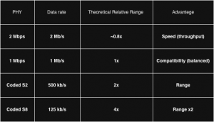
Table of compare between the variants of BLE
The symbol rate in BLE defines the number of modulation symbols transmitted per second at the physical layer and is expressed in symbols per second (sym/s). In BLE 1M and 2M PHY modes, Gaussian Frequency Shift Keying (GFSK) modulation is employed, where each symbol represents one bit of information. As a result, the symbol rate is numerically equal to the nominal PHY date rate. Specifically, the 1M PHY operates at a symbol rate of 1 Msym/s, while the 2M PHY operates 2Msym/s. Increasing the symbol rate directly increases the nominal transmission speed; however, it also reduces receiver sensitivity and shortens the effective communication range, making higher symbol rates more susceptible to noise and interference.
3. BLE Data Transfer Speed Demo Using an IoT Project
To understand BLE more clearly, we started to create a demo using Bluetooth Low Energy in IoT to record with IoS standard and Android standard. The demo system is built around the Nordic Semi- conductor nRF52840, a BLE 5.0 – capable SoC supporting 1M and 2M PHY, Data Length Extension (DLE) and extended MTU sizes. The nRF52840 operates as a BLE peripheral, while smartphones running iOS and Android act as BLE central devices. On the embedded side, the firmware is developed using the Nordic SDK or Zephyr RTOS BLE stack, which allows fine-grained control over PHY mode, connection parameters, and GATT behavior. On the mobile side, the demo application uses CoreBluetooth on iOS and the Android BLE API on Android to receive data from the peripheral.
The experimental results show a clear performance difference between iOS and Android under identical peripheral configurations. When connected to Android devices, the BLE link achieves significantly higher throughput, approaching the expected performance for a 2M PHY configuration. In contrast, iOS devices exhibit lower throughput despite successfully negotiating the same MTU size and PHY mode. This difference is primarily attributed to platform-level restrictions in iOS, including limited control over connection interval, stricter notification pacing, and conservative scheduling policies designed to optimize power consumption.
Although both of platforms report the same nominal BLE speed at the PHY level, the effective data rate observed on iOS is substantially lower. This demonstrates that BLE speed alone does not determine real world data transfer performance and highlights the importance of throughput based evaluation.
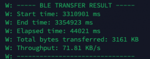
Carry out a survey of throughput on Android
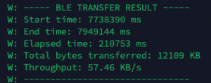
Carry out a survey of throughput on IoS
The results confirm that BLE performance is not solely determined by the peripheral hardware or the BLE specification, but also by the operating system and BLE stack implementation of the central device. Android provides greater flexibility in controlling BLE connection parameters, allowing higher data rates to be achieved. In contrast, iOS abstracts the Link layer and enforces conservative limits to ensure energy efficiency and system stability. These design choices make iOS less suitable for high throughput BLE applications but beneficial for long battery life.
4. Conclusion and Future Improvements for BLE Data Transfer
In conclusion, BLE speed is influenced by many factors beyond the theoretical specifications of Bluetooth Low Energy, including PHY selection, connection interval, packet size, protocol overhead, and the processing capability of the embedded system. While BLE is not designed to compete with high-throughput wireless technologies, it offers an excellent balance between data rate, power consumption, and reliability.
By understanding these limitations and carefully tuning parameters such as MTU size, Data Length Extension, and PHY mode, developers can significantly improve real-world throughput. Ultimately, optimizing BLE speed is not about achieving the maximum possible data rate, but about meeting application requirements efficiently while maintaining low power consumption and stable communication—key priorities in industrial embedded and IoT systems.

